|
|
|
|
Main Menu |
|
|
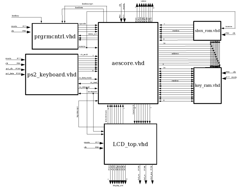
There are 3 main routines implemented to realize the AES algorithm: encryption, decryption, and key expansion routines. The VHDL code is organized into several modules shown in Figure 2. The overall design includes microprogramming concepts and is based on Harvard architecture. Harvard architecture includes separate program and data memory. The memory devices prgrmcntrl.vhd, sbox_rom.vhd, and key_ram.vhd utilize synchronous data transfer. In contrast, the ps2_keyboard.vhd and LCD_top.vhd modules are based on asynchronous data transfer due to the relative speed of the core devices to the lower speed of the HIDs. The sbox_rom.vhd module stores the SBOX and inverse SBOX tables which contain 512 bytes of data, for the substitution box operation referred to in the FIPS197 standard. The key_ram.vhd stores the key expansion, 176 bytes of data, which is calculated from the original 128bit key. This key allows the data to be converted from cipher text to plaintext and visa versa. Prgramcntrl.vhd contains the micro coded instructions of the 3 routines and thus controls the sequential operations of the core. The ps2_keyboard.vhd module decodes the scan codes generated by the keyboard into either ASCII or hexadecimal format for input into the core. LCD_top.vhd displays the user prompts as well as the input and output of the core. |
|
|
|
|
|
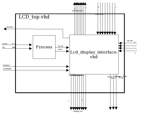
The LCD_top.vhd file contains to main sub system blocks a Process and the lcd_display_interface.vhd. The LCD_top connects the lcd_display_interface.vhd to the entire system. The Process receives the system clock and the resetn signals and uses both signals to create the lcd_clk ouput by use of a counter. The lcd_dislplay_interface.vhd receives the lcd_clk and the reset input from the Process. The lcd_clk is the clock used to drive the state machine within the lcd_display_interface and the reset signal resets the system to an initial state. The asciimode signal is received from the keyboard to determine the display mode to be used by the lcd_display_interface. There are two modes used by the lcd_display_interface one is plain text or ASCII and the second is Hex. The keypress input moves the current data from the output to the input. The core2LCD signal is received for the AEScore which is the data read from memory to be displayed on the LCD. The 4 bit opcode inputs current program status of the system to the display_interface. The inputaccept output sends a signal to the AEScore to allow inputs from the keyboard to be saved in the current memory. The intLCD2Core signal outputs an 8 bit vector to the AEScore to assign the output vector to the core2LCD input signal. The diplay_out 8 bit vector is sent to the LCD RAM along with the lcd_rw, lcd_rs, and nlcd_ena signal to drive the LCD. The lcd_rw, lcd_rs, and nlcd_ena control the LCD display while the display_out signal tells the display which character from the CGRAM memory to display. |
|
|
|
|
|
Reference |
|