SDR Logo

Home
Archives


Project Deliverables

Functional Description
System Block Diagram
Project Proposal
Proposal Presentation
DR Presentation
Final Presentation
Final Report


Related Articles

Project Hardware Kit
802.11a Specifications
Synchronization
Matlab Central


Login

February 2006
SMTWTFS
   1234
567891011
12131415161718
19202122232425
262728    

Valid XHTML 1.0!

Software Defined Radio

Team members: Luke Vercimak, Karl Weyeneth

A software defined radio is a radio transmitter/receiver that uses digital signal processing (DSP) for coding/decoding and modulation/demodulation. This allows much more power and flexibility when choosing and designing modulation and coding techniques. This project will implement a Digital Software radio receiver with a TI C6700 series of digital signal processor.

Due to hardware availability, both the transmitter and receiver will be implemented on the same DSP evaluation board. The system will be constructed and programmed entirely in Simulink using the embedded target for TI C6000 Simulink library. See deliverables for more information.


Tuesday, February 28th

QAM Transmission and Recieving Verification


Using the SRadio Test IN block as the input to the QAM transmitter and receiver system shown in Figure 1, we verified that the data into the system is successfully received on the output. This data is shown in Figure 2.

QAM_trans_rec (7k image)
Figure 1 - The Simulink QAM Transmitter/Reciever Model

QAM_trans_rec_results (25k image)
Figure 2 - The top graph is the input data and the bottom graph is the received output data from Figure 1

The delay in the data shown in the bottom graph of Figure 2 is due to buffering and unbuffering data.
Karl on 02.28.06 @ 08:10 PM CST [link] [No Comments]


Tuesday, February 14th

Complete QAM and OFDM Transmitter/Reciever


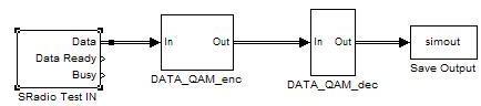
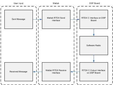
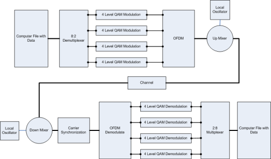
While the test blocks for the DSP board were being developed, work was also being done on integrating the OFDM and QAM designs. Figure 1 shows the overall block diagram for the complete radio. This radio design does not take into account synchronization.

complete_transmitter_reciever (13k image)
Figure 1 - Complete Radio with OFDM and QAM, no synchronization
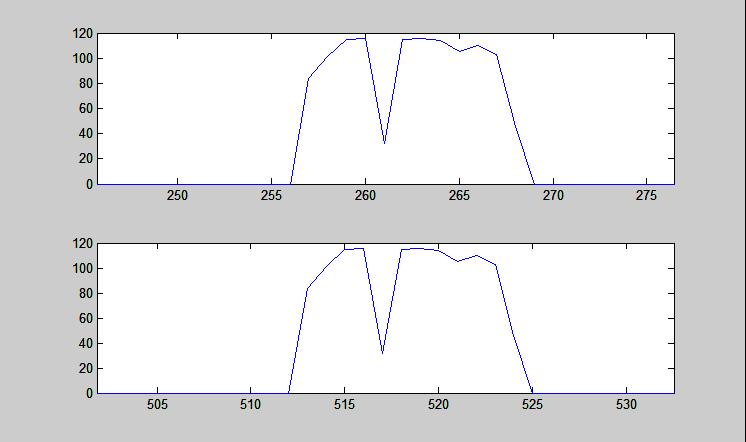
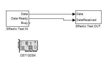
The test data comes from the “Sradio Test IN” block. This block, is the test interface that was developed earlier. It will output data blocks in a 256 byte column arrary. When run in Simulink, the block outputs an initial frame of all zeros then a frame containing the string “Test string.” padded by zeros up to the 256 fame size, and then zeros until the simulation is stopped. The frames are output once per second.

The data then gets QAM encoded, OFDM modulated, interpolated and mixed to a higher frequency of 131.072 KHz. After this it is sent through a channel model (which has no effect for now), demodulated, decimated, OFDM demodulated, QAM decoded and then saved to the Matlab workspace where it can be examined. This design has many different sampling rates which needed to be tracked carefully to ensure a working simulation.

In the QAM modulation block, each byte of the ASCII data gets separated into groups of two bits. Each bit is then mapped onto a 4 level QAM constellation shown in figure 2.

QAM_constellation (4k image)
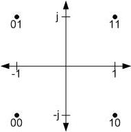
Figure 2 Four Level QAM/QPSK constellation

This constellation was chosen to ease decoding. The MSB is 0 when the real part is negative and 1 when the real part is positive. The LSB is 0 when the imaginary part is negative and 1 when positive.

The QAM data stream needs to be mapped to appropiate OFDM subcarriers. A 64 point IFFT/FFT was chosen for this project because that is what is used in the 802.11a standard. Figure 3 shows the OFDM subcarriers as given by the 802.11a standard.

fft (10k image)
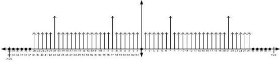
Figure 3 - 802.11a OFDM subcarriers

The subcarrier at 0 or DC is not used so problems with the RF circuitry and ADCs will not occur. Eleven subcarriers are not used on either end of the spectrum to make it practical to filter when upsampling. Pilots are also inserted at carriers -21,-7, 7, and 21 to help with synchronization. Since just 4 QAM symbols are being transmitted at once, only carriers 1,2,3, and 4 will be used at this time. This is shown in figure 4.

fft_2 (6k image)
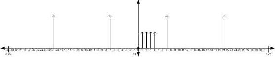
Figure 4 - Project current OFDM subcarrier map


Karl on 02.14.06 @ 04:27 PM CST [link] [No Comments]


Thursday, January 31st

Phase Lock Loop


We are going to be using a phased locked loop for the carrier recovery in the Software radio. Much of this information was researched in "Telecommunication Breakdown" by C. Richard Johnson Jr. To properly recover the carrier, two unknown parameters need to be determined. These are the carrier frequency and phase. Johnson describes how the carrier frequency and phase can be recovered using either a cascaded phased locked loop or a single phased locked loop with a higher order fileter inside a single PLL. If properly chosen, it was indicated that this PLL can track modest frequency and phase changes. The choice for this filter is supposed to be detailed in the document Analysis of the Phased Locked Loop in the CD that came with the book.

In the document Analysis of the Phased Locked Loop proof that the PLL converges when simplified linearly. However, there was little discussion of filter choice for a single PLL that tracks both phase and frequency.

A descrete phased lock loop was created out of signal processing blocks in simulink and see how it reacted to modest changes in frequency and phase.

The following test plots in Simulink verify the design.
PLL_results (44k image)
Figure 1 PLL Simulation Results
The two top graphs in figure 1 are the input and output of the PLL respectively. The bottom graph is the input to the VCO. This is consistant with the behavior of a locked PLL. When the frequency difference is increased to 1 Hz.

PLL_cycle_slipping (17k image)
Figure 2 – PLL that is cycle slipping

One hertz is evidentally beyond the capture range for the PLL. More studying will have to be made to determine how the gain block, filter gain, and VCO sensitivity affect the hold-in and capture range of the VCO.

Karl on 01.31.06 @ 09:22 PM CST [link] [39 Comments]


Thursday, January 26th

RTDX Interfacing and Testing III


Now that the Matlab testing interface was verified using the testing program, the next step is to design the testing software for the DSP side of the board.

The testing software for the DSP board has 3 parts; initialization, data receiving, and data sending. The DSP board timer controls the execution of the Software Radio processing. The timer is disabled when waiting to receive, receiving, and sending data because there is no software radio data processing that needs to be done at these locations. Also, the simulink program is set to abort on an “overrun.” Although this is supposed to be able to be disabled from the “Configuration Parameters” dialog in Simulink.

To test the testing interface, the following simulink block diagram program was created.
RTDX_test_interface_sim (8k image)
Figure 1 - Test program for the simulink interface

This interface was then compiled and downloaded on the board. When working it gives the following response:

Press return to try again. Type exit and return to exit:
Test Message: Test message 1

msg =

Test message 1

Message sent, waiting 5 seconds for it to return

num_msg =

1


outdata =

Test message 1

Press return to try again. Type exit and return to exit:


This is the output of the matlab program. Since the same data coming out is what is going in, the program is working successfully.
Karl on 01.26.06 @ 09:00 PM CST [link] [32 Comments]


Thursday, January 19th

RTDX Interfacing and Testing II


Now that the receive RTDX blocks in Simulink are verified to work and experience has been gained in working with RTDX, Matlab, and Code Composer Studio, we need to design a test system that will verify that the Software radio parts are working as intended on the board. The first thing that needs developed when doing this is a block diagram of the radio. This is shown in Figure 1.
RTDX_block_diagram (17k image)
Figure 1 - Block Diagram for Software Radio Test Interface
The Matlab program will act as the bridge between the user and the DSP board. It will take the user’s “message”, convert the message into a binary stream, transmit it to the DSP board, and indicate to the DSP board that the data is ready to be sent through the radio. On the receive side, the Matlab program will do the opposite. It will wait until DSP indicates that the radio is done processing the data, receive this data into Matlab, and then convert it back into the form of the original message.

On the DSP side, two simulink blocks/sections of C code will interface the RTDX to the software radio designed in simulink. The Input interface block waits until the data has been sent by the Matlab program, the data is put in a convenient location for the Simulink program to process and indicate to the radio that it has data to process. After this, the radio will process the data. The output interface block will stop the radio when its buffer is full and indicate to the Matlab program that the processing has been completed, and transmit the data back into Matlab.

To test the interface, a program will be developed to run on the DSP board. A simple echo program was designed in C to echo back whatever string came in the input of the DSP board. The code from this program will later be used to implement the testing blocks in simulink. A flow chart for this program can be found in figure 2.
RTDX_test_proj_flow (12k image)
Figure 5 - Flowchart for test echo DSP program


Karl on 01.19.06 @ 06:56 PM CST [link] [No Comments]


Thursday, January 11th

RTDX Interfacing and Testing I


The RTDX interface in Simulink was investigated to verify the transfer of data to and from the DSP board when testing the software radio. RTDX is a way to programmatically send and receive data to and from the TI 6713DSK board through code composer studio. Although the interface will not work in a production environment, it is an excellent way to send data to the DSK board for testing.

simulink_rtdx_blocks (11k image)
Figure 1 - RTDX Blocks in simulink

The “From RTDX” block receives data from the host PC and transmits that data to the DSK board. The “To RTDX” block transmits data from the DSK board to the Host PC.

As a starting point for testing, the model in figure 2 was created.
RTDX_test_model (16k image)
Figure 2 - Test model for RTDX data tranmission from DSK to PC

The model counts from 0 – 15, incrementing every 1 second and transmits this to the RTDX channel. This value is also sent to the LEDs so that there is a visual indicator on the board that it is still running the program.

Communication on the host side was programmed in Matlab. The Code Composer Studio link for Matlab provides functions for interfacing with RTDX.
When receiving an RTDX “message” in matbab, there are 3 things one needs to first do:

1. Enable RTDX overall
2. Open the specific RTDX channel.
3. Enable the specific RTDX channel.

Once this takes place, the board will begin to transmit the data to code composer studio. When the connection is not enabled, the messages are lost. The message is then read with the readmsg function. After the data is taken in, the channel is then disabled, closed, and rtdx itself is disabled.


Karl on 01.11.06 @ 03:42 PM CST [link] [No Comments]


Saturday, November 12th

Thoughts on system block diagram and flow of project


After doing some research in Telecommunication Breakdown by C. Richard Johnson Jr. and William A. Sethares, I think there needs some revision to the system level block diagram that is being currently worked on:

System_Block_diagram (33k image)

The transmitter portion of the system block diagram is almost correct. The level of each block is not quite the same but it shows the dataflow through the system. Pulse shaping, if anything, could be added before the QAM modulator to make better use of the bandwidth of each channel. The need for this will depend on the implementation of OFDM and needs to be researched.

The transmitter needs a couple of additions, depending on the amount of corruption that is used in the channel model. Initially we should have complete control over the channel model used. A complete model would add a varible gain/attenuation, delay due to the channel, multipath interference, and interference from other sources. Once an ideal transmitter/receiver is working, these interferences will be added one at a time. The most important interference is the delay of the signal.

Delaying the transmitted signal will make synchronization necessary in the receiver. This is a major part of the project. The block diagram already shows carrier synchronization. This will align the phase and frequency of the transmitter and receiver. However, there are two additional forms of synchronization that need to be considered. These are symbol synchronization and frame synchronization. Symbol synchronization is sampling each pulse at the right moment to ensure the data is extracted from the pulse most accurately. This will extract the 1s and 0s out of the stream. Frame synchronization is knowing when the messages stops and ends in these 1s and 0s. This is important because an offset of just one bit will throw the whole message off. This could be implemented by looking for a known sequence, but there are issues that need to be considered with this also.

After the project works with the channel model in place with all the necessary corruption models, it can be replaced with running the signal out through the D/A converter and back in through the D/A converter. Various corruptions can be done between the D/A and A/D converters, eventually targeting radio frequency circuitry and possibly an antenna.

Preliminary steps/phases for the project can be summarized below (assuming full project completion):
1. Research transmitter/receiver design
2. Design and simulate an ideal transmitter/receiver pair (no channel corruption) and implement on DSP board.
3. Add delay to the channel model and get the 3 levels of synchronization working in simulation. Implement on DSP board.
4. Add other channel corruptions (gain/attenuation and multipath). Verify operation of radio in simulation and on DSP.
5. Remove channel model and run signal through D/A and A/D. Verify operation of radio on DSP board.
6. Introduce interference to physical signal and verify operation.
7. Procure RF circuitry and look into actual wireless transmission.


Luke on 11.12.05 @ 02:07 PM CST [link] [1 Comment]


Friday, November 11th

First Post


This is the first post for the project log. More will come here about the week's progress and activities. Plans for future weeks and such will also be made here.
Luke on 11.11.05 @ 07:11 PM CST [link] [36 Comments]