![]()
|
|
|
|
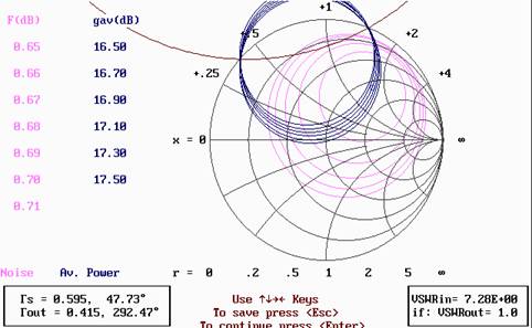
The low noise amplifier(LNA) is one of the major components of the receiver subsystem. The low noise amplifier is to be designed entirely. The transistor to be used for the design of the amplifier will be chosen based on manufacturer specifications and desired specifications depending on the needs of the system. The clarity of the picture output at the TV monitor and the range of the system are determined by the effective of the LNA design specifications. The LNA is to be designed for minimum noise figure for maximum stable gain. The preliminary design of the amplifier are that of the amplifier which was used to make the demo system for the measurements. After evaluating different transistors based on their gain for noise figure specifications, the NE34018 GaAs transistor manufactured by CEL was chosen based on its high gain for a very low noise figure. The Lumped component approach was used to design the transistor circuitry. A software program called CAMAD was used to design the lumped component matching network from the S-parameters and noise parameters of the transistor at the operating frequency. The available power circles and the corresponding noise figure circles for the NE34018 transistor can be seen in the Figure 1 . The voltage reflection co-efficients (Γin and Γ*out ) obtained from those circles are used to find the component values of the lumped components to be used for the matching network to obtain the desired amplifier specifications.
Figure 1 Avalaible gain and the corresponding gain circles
Since a high gain low noise amplifier was needed to improve the range of the system, it was decided to design a two-stage amplifier. The first stage of the amplifier was to be designed for minimal noise and maximum available gain, while the second stage was to be designed just for maximum available gain. The voltage reflection co-efficients (Γin and Γ*out ) obtained for the second stage from the gain circles are shown below in Figure 2 .
Figure 2 2nd stage available gain circles and corresponding noise figure circles
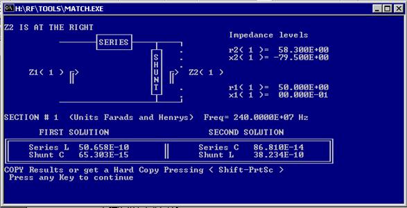
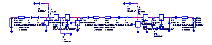
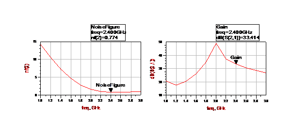
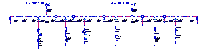
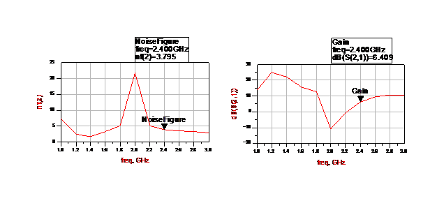
A transistor amplifier circuit with the respective components was constructed in ADS simulation software. The ADS is used to simulate the amplifier outputs and to tune and optimize the circuit. The simulation results obtained through the software are very realistic. Initially the amplifier circuit was built and simulated with the transistor and lumped components only. The schematic diagram of the design and the simulation results are shown as Figure 3 and Figure 4 respectively. After obtaining the desired results, 50 ohm lines were then added to interconnect components. The schematic of the design and the simulation results after adding the 50 ohm lines can be seen in Figure 5 and Figure 6 respectively.
Figure 3 Schematic of the Initial amplifier design
Figure 4 Simulation results for initial design
Figure 5 Schematic of the amplifier after adding the 50 ohm transmission lines to interconnect components
Figure 6 Output simulation of the overall design of amplifier
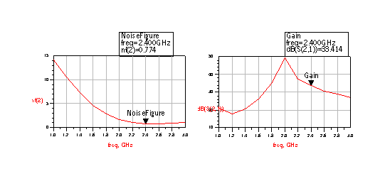
As it can be seen from the Figure 4 and Figure 6, the outputs change drastically. The change occurs due to the inductance and capacitance associated with each of those transmission lines used to inter-connect components. The lumped components values are to be optimized and tuned according to the desired changes in the output. The simulation and tuning tools from ADS can be used to see the changes in the outputs with respect to the change in component values. The lengths of the transmission lines can also be optimized to get the desired outputs. The Figure 7 shows the change in the output curves with respect to the change in component values. All the lengths cannot be changed because they also depend on the size of the components that are to be inter-connected. The final schematic and simulation results can be seen in Figure 8 and Figure 9 .
Figure 7 The change in the output curves as a result of tuning and optimization of different component values
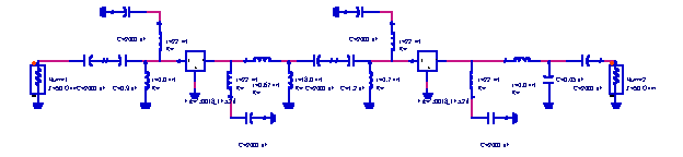
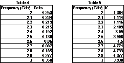
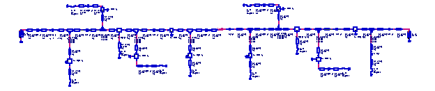
After making the changes to the component values and the lenghts of the transmission lines with respect to the desired outputs the final output simulation results are shown in FIGURE . The stability parameters, K and D are shown in table 5 and table 6 show that the amplifier is unconditionally stable in the operating range. The layout of the amplifier can be seen in Figure 9.The layout takes into consideration the dimensions of all components of the circuit. The components will be mounted on the layout to get the final amplifier circuit. The circuit will then be tested before being used as a part of the WSS.
Figure 8 Final output simulation for the amplifier design
Stability Parameters
Figure 9 Layout of the Low noise amplifier
|
|
|