
|
|
Wireless Terminal and PC Interface using VLSI |
|
|
Wireless Terminal and PC interface using VLSI
Project Proposal
Advisor: Dr. V. Prasad
Date: 12/13/01 Summary Wireless communication systems have gained large success over the last few years, stemming from an increase in technology and refined manufacturing processes. This project will incorporate low-level system design and interface between a host computer via the ISA (Industry Standard Architecture) bus and a wireless RF module. In order to accomplish this task, research must be completed on the ISA bus specifications as well as the wireless device of our choice. Most of the ISA bus architecture research has already been completed through the EE565 ISA design project. Research must also be done on which device will most nearly fit our design specifications, including cost, availability, legality, range, and support. This project will be a small part of a larger design for a wireless interface of some sort. Our design could be used as an interface for a wireless terminal, pager, low-speed network between computers, as well as a host of other applications. Although the terminal may be irrelevant to the project, design considerations will be made surrounding this idea. Narrative
The basic premise behind the ISA interface can be seen in the block diagram below, Fig.1. 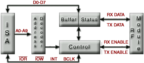 Fig. 1 - Block diagram of VLSI interface chip
From the computer (ISA) side of the interface, all communications will be controlled by the host computer. All action from the ISA side is initiated when a valid address is detected by the chip. Depending then on whether the read or write line is asserted, the appropriate action will be taken. Data will either be written to or read from the internal buffer. If the buffer is full or empty, host intervention is required and an interrupt will be asserted to call attention to the chip. Once the host is alerted, it can then read the contents of the status register to determine whether the buffer is full, empty, or if an error has occurred. The hardware flow chart describes this process quite clearly in Fig. 2. 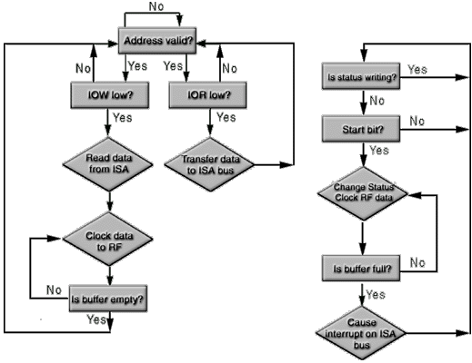 Fig. 2 - Hardware Flow Chart All data flow control as well as error detection and correction will be done in software on the host computer. This eliminates the need for hardware control and correction, which simplifies the design. One of the more difficult tasks in designing the interface will involve timing. Since all signals must be present for a set number of nanoseconds according to the ISA bus standards, careful consideration must be made to ensure all of these times are met with a certain precision. The RF module must also be chosen with a few characteristics in mind. Obviously, cost is an issue, since our project is on a limited budget. If this project were to be considered for manufacture, cost would also be a large issue. Range is another important factor in choosing a module. Practically speaking, a typical home is no more than a few hundred meters from its farthest points. However, if this system were to be used on a college campus, even one as small as Bradley's, the range would need to be significantly more. Support is also another important factor. When a problem arises in the design and testing phases, especially considering the relatively short time span of the project, a solution must be compromised. Preliminary Work A majority of the work involved in this project will revolve around the ISA bus. Luckily, some experience has been gained from EE565, where an ISA design was completed. The inner details of bus timing, loading, and addressing have already been addressed in a similar fashion to that required of this project. Another major aspect will involve having a large variety of transistor gates to "cut and paste" into our final design, following the gate level design. Much of this work has been completed in EE563, VLSI, with Dr. V. Prasad, the project advisor. Certainly the project members will gain an extreme insight into PSPICE, Logic Works, and LEDIT. Much research has also been done in which RF module will best suit the project. The less expensive modules involve a serial data form, with particular encoding, where the more expensive modules have parallel output and handshaking built in. Both have advantages and disadvantages. Future Work In the very near future, a part list must be submitted to order the appropriate parts. The only major component of our project involves the RF module. Therefore, a module must be chosen very soon. After that, the first major step in the design will be at the gate level. This may be done on a number of tools, however, a logical choice would be a software package which would allow for easy implementation on an FPGA. In this manner, our gate level design can easily be tested before and during the transistor-level design. This is another way to physically test our design, rather than rely on computer simulations. After design is complete and testing is accomplished, our final goal will be to draw our design at the transistor level. Most likely, this will be done using LEDIT and PSPICE to test the design one piece at a time. Our preliminary time table can be seen below.
Fig. 3 - Time Table Equipment List The majority of the project will only require a workstation to draw the various aspects of the design at the gate level and at the transistor level. As the project progresses, an FPGA chip will be required to test our design. Basic lab equipment will also be necessary to check the functionality of the design on the FPGA chip. Eventually, as our project nears completion, we will need to test it with the RF module chosen for the design. If confidence is high in the project, an old PC may be used to physically test the design using the FPGA chip. References and Progress For a list of references and to check on the progress of the project, point your browser to:
| |||||||||||||||||||||||