|
|
Wireless Terminal and PC Interface using VLSI |
|
|
Addressing:The standards for the ISA bus set aside a block of addresses for prototyping. This block ranges between 300h and 31Fh and can be addressed using A0-A9. We will require two addresses for this design: a data RX/TX address and a status address. Since no address in the prototype range has no apparent advantage over another, we will use 300h for our data address and 302h for our status address.Why will we not use 301h for our status address? Our interface will be using only 8 bit transmissions. Using Table 1 below, it can be seen that A0, the least significant of the address lines, must be 0 for 8 bit data transmissions on the lower 8 data lines (D0-D7) or 1 for 8 bit data transmissions on the upper 8 data lines (D8-D15). This means that our 8 bit system must have addresses spaced in increments of two. Since we chose 300h for the RX/TX address, the status address must be 302h, 304h, 306h, or any other even value within the prototype range. 302h seems to be the most obvious choice since the RX/TX and status addresses will only differ by a change in A1.
Table 1: Data Bus Addressing Mode Configuration
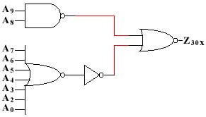
300 (hex) = 1100000000 (binary), so A9=A8=1, and A7=A6=...=A0=0 Figure 1 is the simplest form of the addressing logic in terms of the number of transistors and the area required in a VLSI chip. For a brief explanation of the derivation of the form shown in Figure 1, see the Addressing Logic Explanation page.
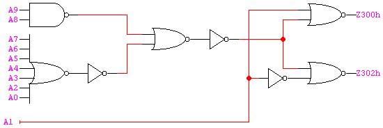 Figure 2: Simplest Addressing Logic for 300h and 302h The necessary components were added to Figure 1 to make the distinction between 300h and 302h. Four additional gates were required: 2 NOR + 2 inverters. The final addressing logic is shown in Figure 2, where
The logic shown in Figure 2 was tested in LogicWorks. The circuit in Figure 2 can be downloaded in the LogicWorks .cct format from the Downloads page. As a final step, BHE' is added to Figure 2 as indicated in Table 1. Since BHE' should be a logic '1' for our desired addressing mode, it is added to the upper NAND gate (refer to the Addressing Logic Explanation page). See Figure 3 for this addition and the final addressing logic.
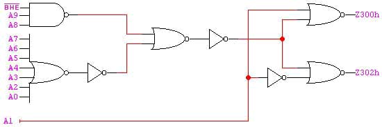 Figure 3: Final Addressing Logic for 300h and 302h with BHE' |