|
Home
Project
Proposal
Addressing
Resources
Bios
Portfolio
Sitemap
|
|
|
Addressing Logic Explanation
**The gate numbers used on this page are based on an address of 300h**
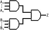
Figure 1: Step 1 of Addressing Logic
|
It should be seen easily that for any address, the basic form of logic used is as seen in Figure 1, where:
- A0...An are the address lines that are required to be logic '1'
- B0...Bn are the address lines that are required to be logic '0'
- Z is the output of the addressing logic
|
For example, in an eight bit addressing scheme, address 210h = 11010010 in binary. Therefore, - A0...An would be bits 1,4,6, and 7
- B0...Bn would be bits 0,2,3,and 5
where bit 0 is the least significant bit.
The configuration in Figure 1, with our 10 bit addressing would require 14 gates. Noting that a AND gate is actually a NAND gate with an inverter (see the gate layouts in .jpg format on the Downloads page), the three logic gates seen in Figure 1 would require 3 NAND gates and 3 inverters. In addition, each input of the B0...Bn gate would require its own inverter, adding 8 inverters. 3 NAND + 3 inverters + 8 inverters = 14 total gates.
|
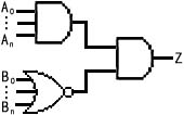
Figure 2: Step 2 of Addressing Logic
|
A large accomplishment is made in Figure 2 (Step 2) by realizing that a AND gate with all of its inputs inverted is the same as a NOR gate. The total number of gates in Figure 2, while obtaining the same output as Figure 1, is only 2 NAND + 2 inverters + 1 NOR = 5 total gates, a reduction of 9 from Figure 1.
|
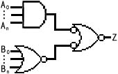
Figure 3: Step 3 of Addressing Logic
|
Again realizing that a AND gate requires a NAND gate and an inverter, one can replace the output AND gate with a NOR gate. To do so, the inputs to the new NOR gate must be inverted, as seen in Figure 3.
|
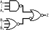
Figure 4: Step 4 of Addressing Logic
|
By completing Step 4, the input AND gate is converted to a NAND gate. The total number of gates in Figure 4 is 1 NAND + 2 NOR + 1 inverter = 4 total gates, which is a reduction of 1 gate from Figure 2 and a reduction of 10 gates from Figure 1.
|
Back to Addressing
|