Project Summary:
The senior project, chosen by Dr. Vinod Prasad, is to design a four-bit arithmetic logic unit (ALU) for a Reduced Instruction Set Computing (RISC) processor. Aida Todri and Kyle Wilken are in charge of designing the control unit, Ricardo Gonzalez is designing the registers, and the memory portion of the project will be designed by Ryan Moffitt and Nandor Toth. All designs will be developed in Ledit and VHDL and then fabricated in FPGA. When all the separate units are complete they will be put together to make the full RISC processor.Narrative:
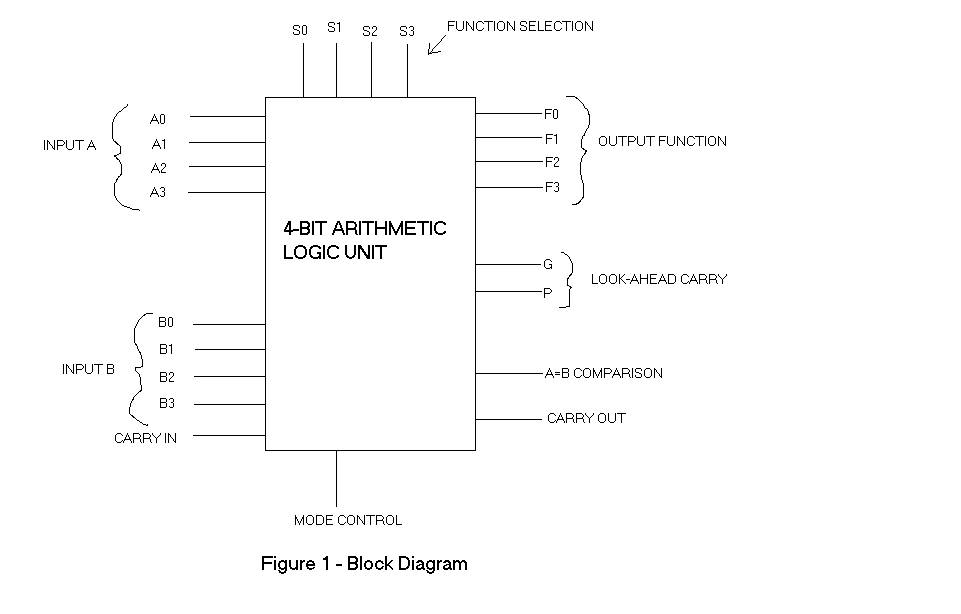
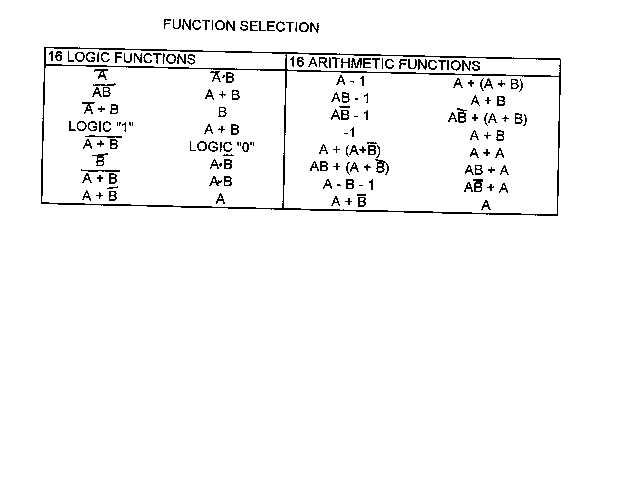
The block diagram, seen in Figure 1 of page 4, shows that the system will be a four-bit ALU that will perform sixteen different logic functions and sixteen different arithmetic functions on two four-bit inputs. The ALU will generate a four-bit output, a comparison of the two four-bit inputs, a carry in signal, and a carry out signal. The mode control will be what is responsible in differentiating between logic functions or arithmetic functions. This can be set to either 0 or 1 to switch between both types of functions.The four different function selection bits, S0-S3, will determine which of the sixteen logic functions or sixteen arithmetic functions will be performed. This will make the ALU capable of carrying out thirty-two different functions. A table showing the functions of the ALU is in Figure 2 on page 5. The table shows various operations which are signified by a +, used to add in the arithmetic functions and used to OR and Exclusive OR in the logic functions, signified by a - for subtraction in arithmetic functions, letters next to each other show multiplication, dots between letters show a logic AND, and bars above letters show them being complemented. These basic functions all have to be taken into consideration when designing and implementing the ALU.
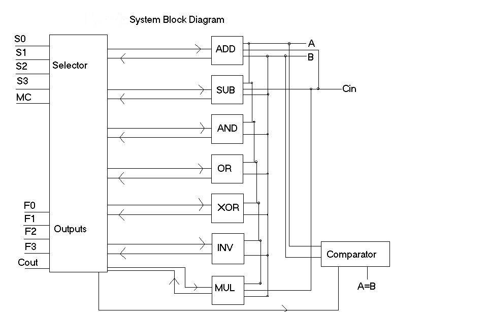
After the desired function is chosen, the selector activates the function or functions that give the desired output. These functions are add, subtract, and, or, xor, invert, multiply, and compare. The block diagram showing this is in Figure 3, on page 6. The add block simply adds the four-bit value from A with the four-bit value of B. This can also be combined with other blocks to add inverted values or other multiple functions. The subtract block takes A and subtracts it with B. The and, or, and xor logic blocks take the binary number from A and performs the logic function with B. The inverter inverts A, B, or both. The multiplier takes A and multiplies it with B. The comparator takes the value of A and B and returns a logic 1 if they are equal; otherwise, it will return a 0.
To be able to perform proper arithmetic functions, the ALU has a carry in (Cin) and carry out (Cout) pin that can be used to incorporate full carry look ahead and provides for either ripple carry between devices using the Cout pin. The Cout pin can also be used with the comparator to indicate A>B or A<B.The circuit will be divided equally among Adem and Chris. Since there are thirty two different functions, the sixteen arithmetic functions will be given to Adem for design, and the sixteen logic functions will be Chriss project. Figure 4, on page 7, illustrates the project outlook for all parts of the ALU design. The first step is to design truth tables and K-maps of each function to be able to design a circuit that can perform the desired task. Next, there is a hand written schematic of the gate level design. This is the general sketch of what the circuit should look like and how to lay it out. After all is completed, the next step is to simplify the circuits into one large circuit using logic works. Next, the layout is entered into Ledit to produce a CAD schematic of the gate level design. With the layout on Ledit, errors can be checked and then compiled into a .cir file so the outputs can be displayed on PSPICE. Once the outputs are shown in the desired fashion, the .cir file will be converted to a Project.cif file, which is the instruction set on building the actual chip. This is sent to MOSIS who designs the chip and sends the final product for final testing. Also with the gate level design a VHDL file can be made which is code that describes the ALUs functions. This can be simulated in Mentor Graphics to find errors and design problems. From this the VHDL schematic is then used to program the FPGA chip to be used for final testing. The final result will be two chips, one designed with code and the other designed with CAD.