The 4-bit arithmetic logic unit (ALU) can perform all 16 logic functions and 16 arithmetic functions depending on the function select inputs. In figure 1, on page 3, bits S0-S3 are the select inputs. When inputted into the selector, the selector generates the desired arithmetic or logic functions. Since there are only 16 possible selections between the select inputs, a mode control input (MC) selects either the 16 logic functions or the 16 arithmetic functions depending on if it is high or low.After the desired function is chosen, the selector activates the function or functions that give the desired output. These functions are add, subtract, and, or, xor, invert, multiply, and compare. The add block simply adds the 4 bit value from A with the 4 bit value of B. This can also be combined with other blocks to add inverted values or other multiple functions. The subtract block take A and subtracts it with B. The and, or, and xor logic blocks take the binary number from A and performs the logic gate with B. The inverter inverts A, B, or both. The multiplier takes A and multiplies it with B. The comparator takes the value of A and B and returns a logic 1 if they are equal, otherwise it will return a 0.
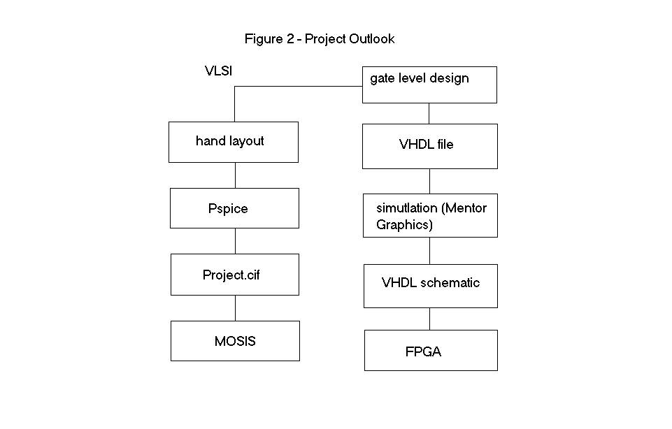
To be able to perform proper arithmetic functions, the ALU has a carry in (Cin) and carry out (Cout) pin that can be used to incorporate full carry look ahead and provides for either ripple carry between devices using the Cout pin. The Cout pin can also be used with the comparator to indicate A>B or A<B.Figure 2, on page 4, illustrates the project outlook for all parts of the ALU design. First, there is a hand written schematic of the gate level design. This is the general sketch of what the circuit should look like and how to lay it out. Next the layout is entered into Ledit to produce a CAD schematic of the gate level design. With the layout on Ledit, errors can be checked and then compiled into a .cir file so the outputs can be displayed on PSPICE. Once the outputs are shown in the desired fashion, the .cir file will be converted to a Project.cif file, which is the instruction set on building the actual chip. This is sent to MOSIS who designs the chip and sends the final product for final testing. Also with the gate level design a VHDL file can be made which is code that describes the ALUs functions. This can be simulated in Mentor Graphics to find errors and design problems. From this the VHDL schematic is then used to program the FPGA chip to be used for final testing. The final result will be two chips, one designed with code and the other designed with CAD.