I/O Design for RISC Microprocessor
By
Eric J. Schultz
Submitted to:
Dr. Vinod Prasad
EE451 Senior Laboratory I
On
November 8, 2000
Project Summary
The objective of this project is to design the Input-Output sections of a RISC (Reduced Instruction Set) processor that is being designed in five distinct parts by five design groups all overseen by Dr. Vinod Prasad. The Input-Output of a processor is an interface to the processor which allows for data to be communicated with devices that are outside the processor package. The most basic I/O port is a tri-state gate with a driver. These are then collected into sets to create ports.
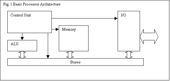
Basic Architecture
The RISC processor consists of a few main sections, these are:
- ALU – Arithmetic Logic unit
- Provides the processor with all of it’s mathematical functions (add, Subtract, Multiply, divide, And, Or….)
- Memory
- Stores Program and data for access by the processor.
- Control Units
- Sends Signals to each section to allow them to work together.
- I/O – Input/Output
- Allows Processor to send signals to external pins.
- Buses
- Paths to allow each main section to transfer data.
Description
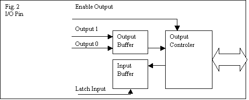
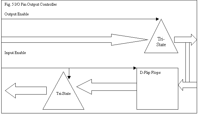
For the I/O section the most basic setup is a pin which can be set high, low, or tri-stated. This is what will first be designed. Secondly A collection of these pins (4 or 8 depending on the bus width.) will be defined for parallel transfers. Others will be defined as both bit and word addressable. All ports will be bi-directional due to the small pin count on FPGA’s. Fig. 2 shows an overview of an I/O pin and Fig. 5 shows detail on the Output Controller part of the I/O pin.
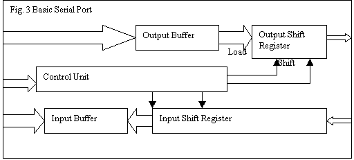
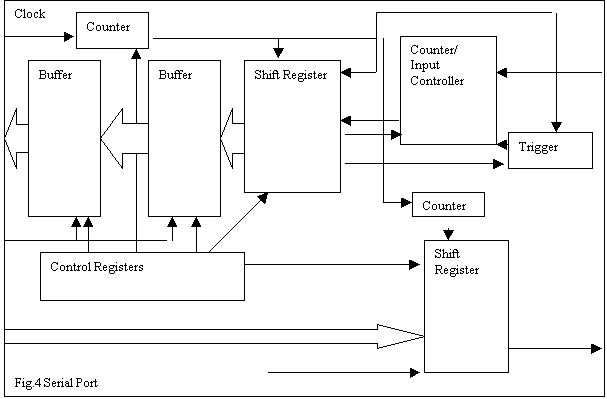
For a serial port, a timer which is available on the FPGA would be used as a baud rate generator. This would drive two shift registers which would be buffered. This would allow an easy interface to the processor. Fig. 3 shows a simplified diagram of the serial port interface. Fig. 4 shows the serial port interface in more detail.