Microcontroller Implementation of a Small Robot Arm Controller
Senior Project May 2000
Department of Electrical and Computer Engineering
Prepared By:
Megan N. Bern
and
Ritesh G. Patel
Advisor:
Dr. Gary L. Dempsey
TABLE OF CONTENTS
Page
Abstract 1
Functional Description 1-2
Complete System Level Block Diagram 3-4
Patents, Standards, & Bibliography 4-5
Datasheet 5-6
Senior Project Demonstration 6-7
Preliminary Laboratory Work 7-27
Hardware 7-17
Interface Circuitry 7-11
Joystick Filter 11-17
Software 17-27
Keil PK51 17-18
Digital Filter 19-21
P Controller 22-25
Menu System 25-27
Suggestions for Fall 2000 27
Appendix: Software Code 28-48
Digital.inc 28
Mod515.inc 29-30
lcddrv3.a51 31-33
Prg4I_df.a51 34-48
Microcontroller Implementation of a Small Robot Arm Controller
Abstract
The project objective was to design and develop an assembly language program for a small robot arm controller using an enhanced 8051 microcontroller (80535). We also designed and constructed the microcontroller interface circuitry and investigated safety features. A keypad and LCD (Liquid Crystal Display) was used to provide a user friendly interface for controller entry and status information. The controller entry and status information is a menu-driven program that eliminates the need for expensive electronic monitoring equipment. The controllers were implemented using an interrupt-driven program.
Functional Description
Our goal for our senior project was to design and develop assembly language and C code for a small robot arm assembly controller using an enhanced 8051 microcontroller (80535). We also designed and constructed the microcontroller interface circuitry, investigated adding safety features such as motor current limit protection, and motor disable hardware/software for excessive position displacements. The add-on keypad and LCD (Liquid Crystal Display) will be used to provide a user friendly interface for controller entry and status information.
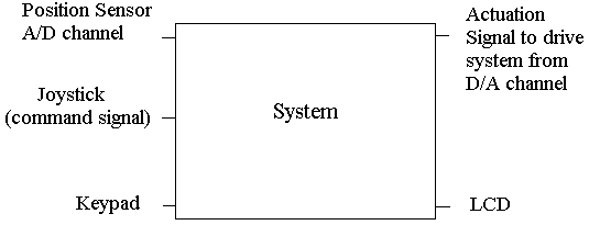
A block diagram of the external input and output signals of the system is shown below in Fig 1. The external input signals consist of the position sensor signal, the signal received from the joystick, and the keypad. The external output signals consist of the actuation signal to drive the system and the LCD.
FIGURE 1:
External Input and Output Signals
INPUTS OUTPUTS
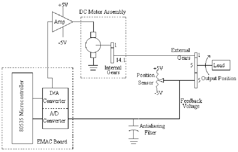
A more detailed block diagram is shown in Fig 2. It includes the microcontroller board, the DC motor assembly, some external gears, a position sensor, and an antialiasing filter. The microcontroller board consists of a keypad, a LCD display, A/D and D/A converters, and the 80535 microcontroller. The microcontroller provides 24 bits of digital I/O, 4 counters/timers, and 10 external interrupts. The microcontroller board is manufactured by EMAC Inc., which is located in Carbondale, IL.
1
The D/A converter output drives the external power amplifier which is connected in a voltage-follower configuration. The amplifier can supply a maximum of 3 Amps to a DC motor. The DC motor converts the control voltage to a mechanical position and velocity. The external gears provide a 70.5 reduction in motor rotor velocity for the external robot arm load. This arrangement is beneficial because the motor "sees" a small load; i.e., the gears step-up torque.
A potentiometer is used for the position sensor. The pot arm is connected to the robot arm via a 1:1 gear. A voltage supply of +/- 5 volts is used for the pot so that the arm position of zero degrees corresponds to zero volts. This feedback voltage which will consist of power supply noise is filtered with a capacitor as the antialiasing filter shown in Fig 2. The combination of the potentiometer resistance and the capacitor is a low-pass filter. The power amplifier, DC motor, gear train, potentiometer, and the
antialiasing filter is part of a system manufactured by Quanser Consulting. The company also provides test software and simple controller software for their system.
FIGURE 2:
Detailed Block Diagram
2
Complete System Level Block Diagram
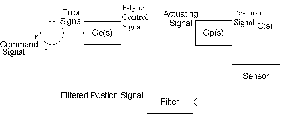
There are also some internal signals that are important for us to evaluate and test. The following signals are available to evaluate on the D/A converter output channels. The control block diagram is shown in Fig 3.
Command signal - Desired robot arm position.
Position signal - Actual robot arm position.
Error signal - Signal = desired position signal - filtered position sensor signal.
P-type controller - The output signal from the PID(proportional+integral+derivative)-type
signal controller.
Filtered position - The filtered actual position sensor signal.
Signal
Actuating signal - Signal that drives the robot arm system, connected to power amplifier.
FIGURE 3 :
Control Block Diagram
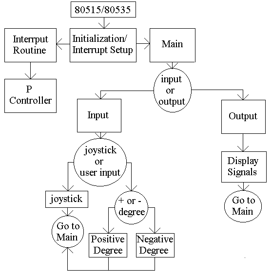
The software flowchart is shown in Fig 4. The software contains an interrupt service routine as well as the main program. The software will check to see if the user would like to select the input to the system or examine the outputs of the controller. If the input is chosen, the software will check if the joystick or user input is desired. If the joystick is desired, the joystick will be the command signal. If the user input is desired, the software will check for a positive or negative degree that is entered on the keypad. The robot
3
arm will then move to the desired degree. If the output is chosen, the software will offer the desired signal to be displayed. Timer 2 of the 80535 microcontroller will be used to generate the interrupt for the P controller calculations. Initially, the timer will be set for a 5 millisecond interrupt (200 Hz sampling). This fast sampling time will make the overall system look like a continuous-time system instead of a discrete-time system. Dr. Dempsey suggested 200 Hz sampling based on previous research.
FIGURE 4:
Software Flowchart
Patents, Standards, & Bibliography
For our project it was suitable to investigate the microcontroller boards that would be used for the control system instead of a patent search. The minimum microcontroller board would consist of an INTEL microcontroller, 4 channels of analog-to-digital converters, 4 channels of digital-to-analog converters, external RAM for user programs, program download capability from a personal computer (PC), a keypad, and an LCD for displaying of status information. The EMAC board meets these requirements, and was selected by our advisor, Dr. Dempsey, for this senior project. Other manufacturers that were evaluated
were Advanced Education Systems (AES) and Rigel Corporation. Over twenty hours were required
searching the World Wide Web for the appropriate vendor. The board from EMAC Inc. was selected based
4
on the hardware features such as external keypad and 2-line LCD. The debugging software system provided is poor, however, this was also the case for the other vendors. The software package called Keil PK51 will be used as a professional debugging package that will work with the EMAC board.
There are no standards that apply to the project because the EMAC board will be used in a standalone manner. However, during development, the EMAC board will connect to an IBM compatible computer. These standards for the computer are shown below in Table 1.
TABLE 1:
List of Standards
1. IBM 486 compatible computer or higher with math CO-processor
2. DOS version 6.2
3. Windows 3.11 or WIN95
Datasheet
The input signal to the control system is shown in Fig 5. The final positions labeled +CMD (command signal) and -CMD are also known as the set points. The velocity is the slope of the waveform. A velocity command of 100° /sec is shown below.
FIGURE 5:
Input Signal to Control System
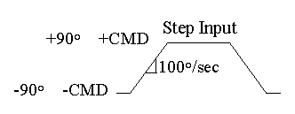
The numerical specifications for the input signal shown above are listed in Table 2.
TABLE 2:
Numerical Specifications for Step Input
1. | CMD | £ 90° .
2. Velocity(max) = 45° /sec.
The outputs of the control system are the position and velocity of the robot arm. The numerical specifications shown in Table 3 will be measured using a Tektronix TDS 340A Oscilloscope. Since we are dealing with frequencies under 1 Hz, measuring these specifications off of the oscilloscope takes hours.
The less time consuming measurements are % O.S., Ts, and tp. The other measurements are measured by finding the Bode plot of the system, which again can take hours.
5
TABLE 3:
Measured Outputs of Control System
POSITION
% O.S. - Percent overshoot @ 5(%).
tp - Time to first peak @ 6(s).
Ts - Settling time @ 9(s).
Mp - Resonant peak @ 1.1.
Wp - Resonant frequency @ 0.16(rad/sec).
BWc.l. - Closed loop bandwidth @ 0.5(rad/sec).
PM - Phase margin @ 69.
GM - Gain margin @ 4.
ess < 2° .
VELOCITY
Tracking error < 2° .
The user interface for this project is the keypad and the LCD. Since the LCD only has two lines to display information, there will be two modes for the LCD. The first mode will be for the user input. This input will be entered through the keypad. Table 4 lists the possible inputs from the user. A help menu will be used to enter these parameters. For example, push 1 on the keypad to turn the motor on or push 0 to turn the motor off.
TABLE 4:
User Inputs
1. Motor ON/OFF.
2. kp gain.
3. Command set point.
4. Ramp velocity.
5. Command frequency.
The second mode for the LCD will be to display some of the signals shown in Fig 3. From a help menu, the user will be able to designate which signal should be displayed in real-time. This will be helpful for system evaluation purposes.
Senior Project Demonstration
For demonstration, the percent overshoot, time to first peak, and settling time will be measured and compared with simulation results from MATLAB. This will be the fastest method to prove our controller
works. Prediction equations can then be used to calculate parameter values in the frequency domain, which can also be compared with simulation results. The equipment needed to perform the demonstration is listed in Table 5.
6
TABLE 5:
Equipment List
Laboratory Work
Hardware: Interface Circuitry
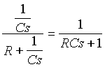
The initial problem was that the potentiometer (position sensor) and the power amplifier that drives the motor operate over a range of +5V to -5V. The analog-to-digital (A/D) and digital-to-analog (D/A) converters only operate over a range of 0V to +5V. The block diagrams shown in Figs 6a and 6b were used as linear models for designing the interface hardware. Tables 6a and 6b list the calculated inputs and outputs for the block diagrams in Figs 6a and 6b.
FIGURE 6a:
Potentiometer Output to A/D Input Block Diagram
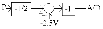
FIGURE 6b:
D/A Output to Power Amplifier Input Block Diagram
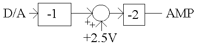
TABLE 6a:
Linear Scale of Potentiometer to A/D
Potentiometer A/D
5V 5V
2.5V 3.75V
0 2.5V
-2.5V 1.25V
-5V 0V
7
TABLE 6b:
Linear Scale of D/A to Power Amplifier
D/A P
5V 5V
3.75V 2.5V
2.5V 0V
1.25V -2.5V
0V -5V
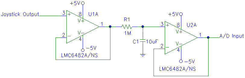
The schematic shown in Fig 7 is the hardware design used to implement the linear conversion needed to interface the potentiometer with the A/D converter. The schematic was built using the LMC6482AIN Dual Rail-To-Rail Input and Output Operational Amplifier. The feature of interest for the LMC6482AIN is that the Rail-To-Rail Output Swing ranges within 20mV of the supply rail with a 100 kW load.
FIGURE 7:
Final P-to-A/D conversion schematic
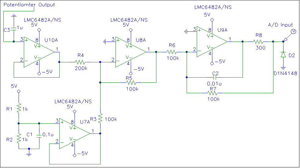
The P-to-A/D conversion schematic contains the antialiasing filter shown in Fig 2. It is placed from the potentiometer output to ground. There was a buffer added to separate the antialiasing filter from the P-to-A/D conversion hardware.
8
We investigated the A/D input impedance to see if there would be any impedance mismatching problems. The specification sheets for the A/D found under H:\Datasheets\MicroPac535\m515.pdf (page 143) listed the following limit values for internal resistance and capacitance. The sampling time used for the digital filter is ts=0.005s. According to the equation listed under max limit values, RASRC=9kW . The internal resistance may not be a problem, but the input capacitance may cause the op-amp to oscillate.
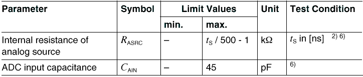
The specification sheets for the LMC6482 rail-to-rail were found at www.national.com/pf/LM/ LMC6482.html#Datasheet. The specifications indicate that the LMC6482 can typically directly drive a 100pF load with Vs=15V at unity gain without oscillating. The unity gain follower is the most sensitive configuration. This was the type of configuration being used. This direct capacitive loading reduces the phase margin of op-amps. The combination of the op-amp’s output impedance and the capacitive load induces phase lag. This results in either an underdamped pulse response or oscillation.
The schematic shown in Fig 8 was suggested by the specification sheets for the LMC6482 to handle a 330pF load. R2 and C1 serve to counteract the loss of phase margin by feeding forward the high frequency component of the output signal back to the amplifiers inverting input, thereby preserving phase margin in the overall feedback loop. The values of R2 and C1 are experimentally determined for the desired pulse response.
FIGURE 8:
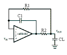
The capacitor CL is the A/D converter input capacitance which is 45pF. The value of R1 is 100kW . The value for C1 was chosen to be 0.01m F. The value for R2 was experimentally chosen. A value of 300W for R2 was chosen for the first test implementing the schematic shown in Fig 8.
The circuit was tested and measured with a FLUKE 45 Dual Display Multimeter EQ-2203. The recorded values are shown in Table 7.
9
TABLE 7:
Inputs vs. Outputs for P-to-A/D
Potentiometer Calculated Experimental
5.00V 5.00V 4.998V
2.50V 3.75V 3.7774V
0.00V 2.50V 2.511V
-2.50V 1.25V 1.249V
-5.00V 0.00V -0.013V
The schematic shown in Fig 9 is the design used to implement the linear conversion needed to interface the D/A converter with the power amplifier.
FIGURE 9:
Final D/A-to-Amp conversion schematic
There was an inverter added to the D/A-to-Amp conversion hardware. This was done to counteract the inverter on the power amplifier. The circuit was tested and measured with a FLUKE 45 Dual Display Multimeter EQ-2203. The recorded values are shown in Table 8.
10
TABLE 8:
Inputs vs. Outputs for D/A-to-Amp
Potentiometer Calculated Experimental
5.00V 5.00V 4.898V
3.75V 2.50V 2.439V
2.50V 0.00V -0.018V
1.25V -2.50V -2.477V
0.00V -5.00V -4.938V
The results shown in Tables 7 and 8 are within 60mV from the desired results, therefore the schematics shown in Figs 7 and 9 were used for the interface circuitry.
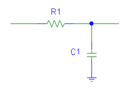
Hardware: Joystick Filter
The joystick signal that will be used as a command signal for the controller for the robot arm needs to be filtered. Without a filter, the command signal causes the D/A converter to saturate and the control system operation would be nonlinear and unpredictable. The tradeoff is the system will be very slow.
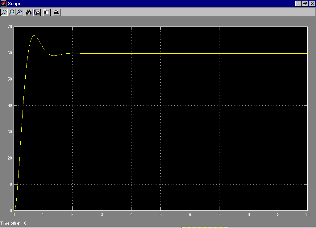
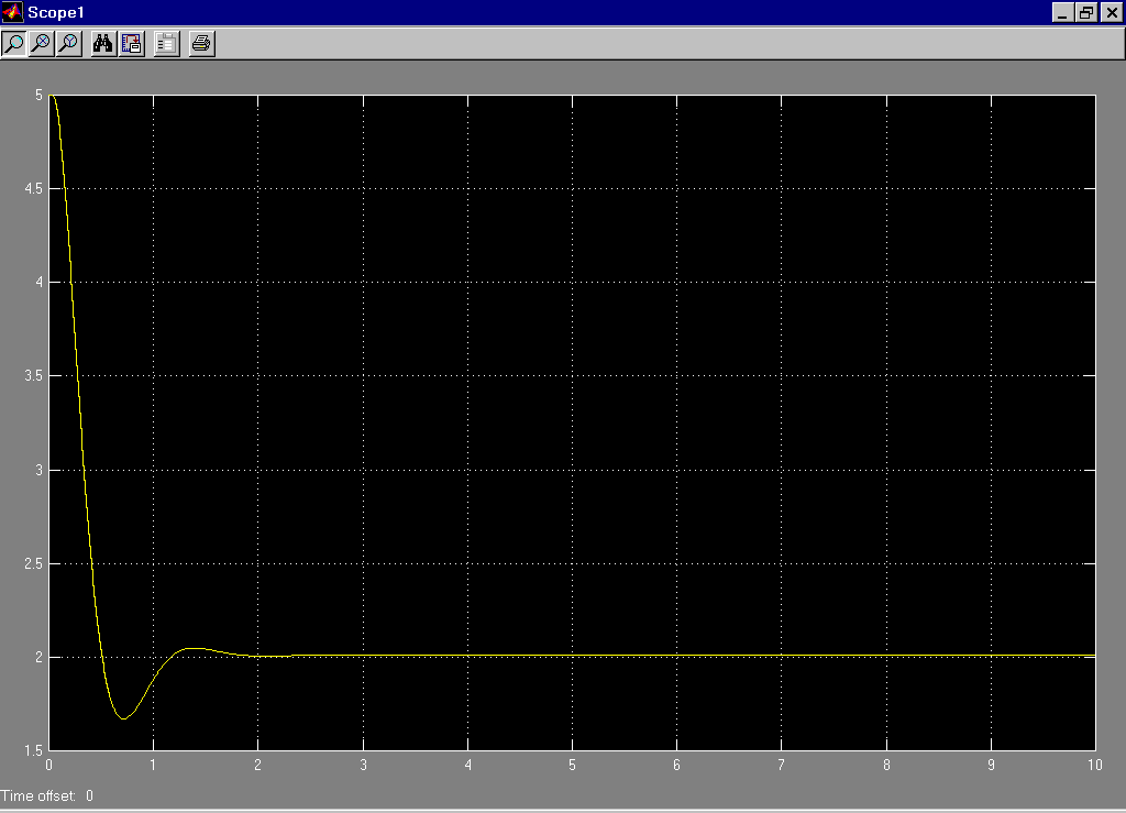
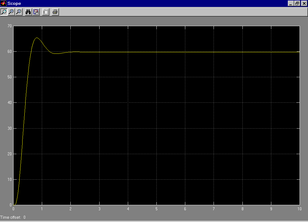
A low-pass filter was used for the joystick. The pole of the low-pass filter shown at the output of the step block in Fig 10 was experimentally chosen using Simulink. Various values for the pole were entered into the simulation and the output of the controller (Scope) and the response before the D/A converter (Scope1) were evaluated.
The results of Scope and Scope1 were looked at before the low-pass filter was added to the system in simulation. Scope and Scope1 are shown in Figs 11 and 12. As you can see from the results, Scope1’s output hits the rail before it settles to 2V. This is something we would like to fix.
The value that we decided to use for the pole was 10 rad/sec. The simulation results with the low-pass filter added in are shown in Figs 13 and 14. The results for Scope1 are much better with the low-pass filter inserted in the simulation. The output is within a safe distance from the rail. The value 10 rad/sec will be the value of the pole implemented in hardware.
FIGURE 10:
Block Diagram for P Controller
11
FIGURE 11:
Scope Results without Low-pass Filter
12
FIGURE 12:
Scope1 Results without Low-pass Filter
13
FIGURE 13:
Scope Results with Low-pass Filter

14
FIGURE 14:
Scope1 Results with Low-pass Filter

The low-pass filter will be represented in hardware as shown in Fig 15. Two buffers are added at the input and output of the LPF to separate the LPF from the joystick output and the A/D converter input. The low-pass filter is represented by (1).
FIGURE 15:
Schematic for Joystick Filter
15
 where 1/RC=pole value (1)
Figure 15 shows the values for R and C which are: R=1MW and C=10m F. These values for R and C give the 10 rad/sec pole that is needed. We measured the components chosen for the hardware using a Hewlett Packard 4261A LCR Meter. The results for the measurements are: R=1.0038MW and C=10.44m F @ 120Hz.
These values were than entered into Fig 10 and simulated using Simulink. The results are shown in Figs 16 and 17. As you can see there is not a significant difference in Scope or Scope1, so these component values were used for the joystick filter.
FIGURE 16:
Scope Results with Measured Component Values
16
FIGURE 17:
Scope1 Results with Measured Component Values

Software: Keil PK51
The documentation to learn Keil PK51 consisted of about 20 pages that was found in the Junior Laboratory. This documentation didn’t show how to start your own project, so a lot of time was wasted trying to figure out how to set up a project within the new software. There was also no documentation on installation of the software available.
The MOD515 program had to be revised. Some of the variables would have been renamed if they were not erased which would cause errors. We also had to rename MOD515.a51 so that Keil PK51 will recognize the file. The digital.asm program was also renamed as digital.a51 for the same reason. These three files were saved in the c:\Temp directory. MOD515.a51 is attached to this report as well as digital.a51, and prg4I_df.a51.
The following steps listed in Table 9 will set up a project for a program, run the program, and interface with the EMAC board.
17
TABLE 9:
Keil PK51 Tutorial
This will run the programs attached to this report.
18
Software: Digital Filter
The following analog filter shown in Fig 18 is a low-pass filter. This filter will be implemented in assembly language to filter the position signal.
FIGURE 18:
Analog Filter
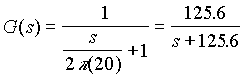
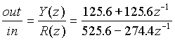
This digital filter is represented by the transfer function shown by (2). The single pole is located at 20 Hz. A 20 Hz pole was chosen so that the 60 Hz noise of the power supply would be filtered and so that the pole of the digital filter would be more than a decade away from the plant double pole.
 (2)
(2)
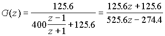
This equation is converted to z-plane form using the Tustin Method (bilinear transformation). The variable s is replaced by (3) where T=fixed sampling period=0.005s. The transfer function in z-plane is shown in (4).

 (4)
(4)
Equation 4 is then divided by the highest power of z giving (5) and (6).
![]() (6)
(6)
19
Taking the inverse z transform gives (7) where yn = current output, yn-1 = past output, rn = current input, and rn-1 = past input.
![]() (7)
(7)
There are 4 internal RAM locations needed for the 4 different variables. Solving for yn gives (8).
![]() (8)
(8)
The steady state value of the filter is 1.0, so (8) should add up to 1.0. Equation 8 is rounded up to (9) to make it easier to write in code. Equation 9 also adds up to 1.0. This equation will be implemented in assembly language.
![]() (9)
(9)
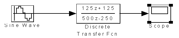
The digital filter was simulated using Simulink. Figure 19 shows the block diagram used for the simulation.
FIGURE 19:
Simulink Block Diagram
By double clicking on the Sine Wave box, a window of parameters is displayed. Table 10 lists the parameters that were used.
TABLE 10:
Sine Wave Parameters
The transfer function G(z) for a 20 Hz pole is
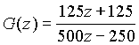 (9)
(9)
20
By double clicking on the Discrete Transfer Fcn box, a window of parameters is displayed. Table 11 lists the parameters that were used.
TABLE 11:
Discrete Transfer Fcn Parameters
The simulation was ran by clicking on simulation and choosing START. After the simulation is done, double clicking on the Scope box will display the results. The results showed that the output is approximately 0.707 of the input signal. This would be the 3dB down point or the pole location, which was designed to be 20Hz.
The code for the digital filter was written to implement (9). The code is included in the Appendix. The remainders for the digital filter had to be included into the current output, yn. The remainders from 0.25rn and 0.25rn-1 were added together. The remainder for 0.50yn-1 had to be multiplied by 2 before added to the other two remainders. Then the total remainders were divided by four and added in to the total for the current output, yn. The digital filter was then tested using Keil PK51. The input to the A/D was a 1Vp-p sine wave with a DC offset of 500mV at a frequency of 20Hz. The output should be 0.707 of the input. The output is shown in Fig 20.
FIGURE 20: Output of Digital Filter @ 20Hz
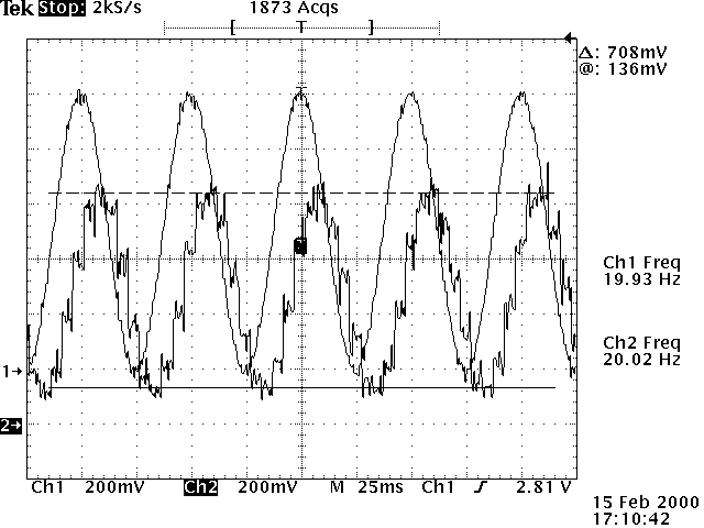
The output versus input shown in Fig 20 proves that our digital filter was working properly.
21
Software: P Controller
The block diagram that represents the P controller for the robot arm system is shown in Fig 21. In the feedback loop of this block diagram the first block on the right is the gain of the potentiometer from the robot arm. This value, 0.02805, is fed into the antialiasing filter, through the P-to-A/D hardware interface, and finally through the digital filter. To avoid any overflow problems that may occur in the feedback path, 80H was subtracted from the output of the digital filter. The 80H will be added back into the system after the summation of the P controller. Then the 2’s compliment was taken of any negative numbers that occurred. The sign of the digital filter output, - or +, was also kept in a RAM location called negf; 1 representing a negative number and 0 representing a positive number. This gain needs to be a gain of 1 before it is manipulated by the Gain K1 block. To achieve a gain of 1, the output of the digital filter is then multiplied by the inverse of the potentiometer gain.
FIGURE 21:
Block Diagram for P Controller
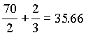
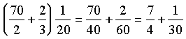
To implement the inverse, 35.66, in software without the use of 16-bit numbers, (10) will be used to represent 35.66. This would then be fed into the Gain K1 (0.05) block. To simplify the assembly language the inverse potentiometer gain and the Gain K1 blocks will be performed at the same time. This can be done by using (11).
22
This brings us to the summation of the P controller. The first step is to get the input command signal. This command signal can either be an input from the joystick or a degree of position chosen by the
user. This will be explained in more detail in the menu system discussion. If the joystick is being used, a 1 will be placed in a RAM location called joy. The input command signal will then feed into an A/D channel and then manipulated from there.
If the user wants to move the robot arm to a specific degree of position, then a 1 will be placed into a RAM location called isig. Depending on the degree of position desired from the user, a hexadecimal value will be used as the input command signal and manipulated from there.
Since 80H was subtracted from the feedback signal, 80H must also be subtracted from the input signal, whether it is the joystick or a user chosen value. Then the 2’s compliment was taken of any negative inputs due to the subtraction. The sign of the input, - or +, was also kept in a RAM location called negi; 1 representing a negative number and 0 representing a positive number.
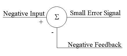
The next step of the summation of the P controller is to consider the four possible cases that may occur. The first case is when the input to the controller is positive and the feedback signal is positive. The second case is when the input to the system is positive and the feedback signal is negative. The third case is when the input to the system is negative and the feedback signal is positive. The fourth case and final case is when the input to the system is negative and the feedback signal is negative.
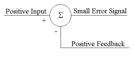
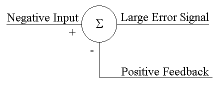
When dealing with the first case, the input signal and the feedback signal both being positive, the diagram shown in Fig 22a shows the condition at the summer of the P controller. A positive feedback signal is subtracted from a positive input signal giving a small error signal causing no overflow or negative number problems even after the 80H is added to the error value.
FIGURE 22a:
Input and Feedback Signal both Positive
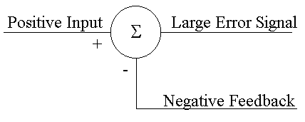
When dealing with the second case, the input signal is positive and the feedback signal is negative, the diagram shown in Fig 22b shows the condition at the summer of the P controller. Subtracting a negative feedback signal from a positive input signal is the same as adding a positive feedback signal to a positive input signal. This was performed in the code since the 2’s compliment was taken of the negative number. This addition can definitely cause an overflow when adding the 80H to the large error signal. This is a condition that we don’t want to occur.
23
FIGURE 22b:
Input Signal Positive and Feedback Signal Negative
When dealing with the third case, the input signal is negative and the feedback signal is positive, the diagram shown in Fig 22c shows the condition at the summer of the P controller. Subtracting a positive feedback signal from a negative input signal is the same as subtracting a positive feedback signal and a positive input signal from 0H. This was performed in the code since the 2’s compliment was taken of the negative number. This addition can definitely cause the case where a negative number is sent to the D/A converter even after 80H is added to the large negative error signal. This is a condition that we don’t want to occur.
FIGURE 22c:
Input Signal Negative and Feedback Signal Positive
When dealing with the forth and final case, the input signal and the feedback signal both being negative, the diagram shown in Fig 22d shows the condition at the summer of the P controller. A negative feedback signal is subtracted from a negative input signal. This is the same as subtracting a positive input signal from a positive feedback signal. This was done in code since the 2’s compliment is taken of all negative numbers. This condition also gives a small error signal causing no overflow or negative number problems even after the 80H is added to the error value.
24
FIGURE 22d:
Input and Feedback Signal both Negative
After the summation occurs in the P controller 80H is added to the error signal. This value is then passed through the D/A converter. This value is then converted from the range of 0V to 5V to a range of 5V to -5V by the D/A-to-Amp converter hardware and sent to the power amplifier. The power amplifier then drives the plant. Then the processes are repeated by sending the value of the potentiometer (position sensor) into the P-to-A/D converter hardware.
It was found that there is a saturation problem with the D/A converter after the summation of the P controller. The 8051 microcontroller was an 8-bit microcontroller and would overflow. The plant was found using a 12-bit A/D and D/A card.
Software: Menu System
The menu system was designed to be a friendly user interface. The menu system will begin with a main menu prompt from the LCD. It will read the following:
Press 1 or 2
1=In 2=Out For Menus
There was a problem at first when trying to implement this main menu prompt. The microcontroller was writing to the LCD way too fast. The problem was solved by using an interrupt to slow down the time each character was sent to the LCD. It was decided that sending a character to the LCD every 0.05 seconds was plenty of time to delay each character. This was successfully written to the LCD.
The code is written to accept only a 1 or a 2 from the keypad. If a 1 is entered from the main menu prompt, the code will jump to a INPUT1 subroutine. If a 2 is entered, the code will jump to a OUTPUT1 subroutine.
Once in the INPUT1 subroutine, the microcontroller will write the following to the LCD:
Press 1 0r 2
1=JOYSTICK 2=INSIG
The code is written to accept only a 1 or a 2 from the keypad.
25
If a 1 is entered, the RAM location called joy will change from a 0 to a 1 and the RAM location called isig will change to 0. The interrupt will check joy and allow the input to an A/D from the joystick if there is a 1. It will then loop back to the main menu prompt and wait for the next input signal choice from the user before it turns the joystick off.
If a 2 is entered, the RAM location called isig will change from a 0 to a 1 and the RAM location called joy will change to 0. The interrupt will check isig and allow the input chosen by the user to be used as the input to the P controller if there is a 1. The following prompt will be displayed as the interrupt continues to run:
1 = Positive Degree
2 = Negative Degree
The microcontroller will only accept a 1 or 2. If a 1 is accepted the following prompt will be displayed:
1=10 2=20 3=30 4=40
5=50 0=other
The microcontroller will only accept a 1, 2, 3, 4, 5, or 0. This value is then saved in the RAM location called isig. If a 1, 2, 3, 4, or 5 is entered, the P controller will recognize what degree the user would like the robot arm to move to by checking the isig RAM location and the robot arm will move to the degree of choice. If a 0 is accepted the following prompt will be displayed:
6=60 7=70
8=80 9=90
The microcontroller will only accept a 6, 7, 8, or 9. This value is then saved in the RAM location called isig. The P controller will recognize what degree the user would like the robot arm to move to by checking the isig RAM location and the robot arm will move to the degree of choice. If the microcontroller accepted a number from 1-9, the main menu prompt will be written to the LCD after the signal to move the robot arm to the degree of choice is sent.
If a 2 is accepted from the input signal prompt, the following prompt will be displayed:
-1=10 -2=20 -3=30
-4=40 -5=50 0=other
The microcontroller will only accept a 1, 2, 3, 4, 5, or 0. If a 1, 2, 3, 4, or 5 is entered, the robot arm will move to the degree of choice as explained for positive numbers. If a 0 is accepted the following prompt will be displayed:
-6=60 -7=70
-8=80 -9=90
The microcontroller will only accept a 6, 7, 8, or 9. The robot arm will then move to the degree of choice.
26
To actually move the robot arm to a specified position degree can be done by finding what voltage level of the robot arm corresponds to the desired degree of position. The desired voltage level is converted into a hexadecimal number. This hexadecimal number is then placed into the RAM location isig for the specified degree of position.
Suggestions for Fall 2000
There is a problem that needs to be fixed before any more code is written. It was found that the included file lcddrv3.a51 uses R2. The digital filter in the P controller also uses R2. This needs to be fixed so that just one of them is using R2.
The verification of the model using an 8-bit A/D and D/A converter would be a good idea. The model for this project was found using 12-bit A/D and D/A converters and was then implemented using 8-bit A/D and D/A converters. This may have been the problem with the D/A saturating after the summation of the P controller.
It is suggested to use a PID controller to reduce steady state error or add an optimum P controller. A Feed-forward controller will make the system faster. It would also be a good idea to use C language for high level software. This will definitely save time to implement other things for the project. Another thing that has to be continued is the menu system. Items such as the output menu implementation, the kill relay, and current limit protection to name a few.
27
Appendix: Software Code
Digital.inc
;***********************************************************************
;
; Include File For Definitions
;
;***********************************************************************
IPAD equ 30H ;Current Input From A/D
IP_1 equ 31H ;Past Input
OP equ 32H ;Current Output
OP_1 equ 33H ;Past Output
Tmr_Half equ 34H ;Half Second Timer
joy equ 35H ;joystick condition
negi equ 36H ;input condition
negf equ 37H ;feedback condition
KEYSEL equ 38H ;KEYPAD PORT
isig equ 39H ;input signal condition
feed equ 40H
comm equ 41h
Rn equ 42h
;d/a
DA_0 Equ 10H
DA_1 Equ 11H
DA_2 Equ 12H
DA_3 Equ 13H
28
Mod515.inc
; 80515 MOD FILE
IEN0 DATA 0A8H ;INTERRUPT ENABLE REGISTER 0
IP0 DATA 0A9H ;INTERRUPT PRIORITY REGISTER 0
IEN1 DATA 0B8H ;INTERRUPT ENABLE REGISTER 1
IP1 DATA 0B9H ;INTERRUPT PRIORITY REGISTER 1
IRCON DATA 0C0H ;INTERRUPT REQUEST CONTROL
CCEN DATA 0C1H ;COMPARE/CAPTURE ENABLE
CCL1 DATA 0C2H ;COMPARE/CAPTURE REGISTER 1 - LOW BYTE
CCH1 DATA 0C3H ;COMPARE/CAPTURE REGISTER 1 - HIGH BYTE
CCL2 DATA 0C4H ;COMPARE/CAPTURE REGISTER 2 - LOW BYTE
CCH2 DATA 0C5H ;COMPARE/CAPTURE REGISTER 2 - HIGH BYTE
CCL3 DATA 0C6H ;COMPARE/CAPTURE REGISTER 3 - LOW BYTE
CCH3 DATA 0C7H ;COMPARE/CAPTURE REGISTER 3 - HIGH BYTE
T2CON DATA 0C8H ;TIMER 2 CONTROL
CRCL DATA 0CAH ;COMPARE/RELOAD/CAPTURE - LOW BYTE
CRCH DATA 0CBH ;COMPARE/RELOAD/CAPTURE - HIGH BYTE
TL2 DATA 0CCH ;TIMER 2 - LOW BYTE
TH2 DATA 0CDH ;TIMER 2 - HIGH BYTE
ADCON DATA 0D8H ;A/D CONVERTER CONTROL
ADDAT DATA 0D9H ;A/D CONVERTER DATA
DAPR DATA 0DAH ;D/A CONVERTER PROGRAM REGISTER
P4 DATA 0E8H ;PORT 4
P5 DATA 0F8H ;PORT 5
INT3 BIT 090H ;P1.0 - EXTERNAL INTERRUPT 3/CAPTURE 0/COMPARE 0
INT4 BIT 091H ;P1.1 - EXTERNAL INTERRUPT 4/CAPTURE 1/COMPARE 1
INT5 BIT 092H ;P1.2 - EXTERNAL INTERRUPT 5/CAPTURE 2/COMPARE 2
INT6 BIT 093H ;P1.3 - EXTERNAL INTERRUPT 6/CAPTURE 3/COMPARE 3
INT2 BIT 094H ;P1.4 - EXTERNAL INTERRUPT 2
T2EX BIT 095H ;P1.5 - TIMER 2 EXTERNAL RELOAD TRIGGER INPUT
CLKOUT BIT 096H ;P1.6 - SYSTEM CLOCK OUTPUT
T2 BIT 097H ;P1.7 - TIMER 2 INPUT
ET2 BIT 0ADH ;IEN0.5 - TIMER 2 INTERRUPT ENABLE
WDT BIT 0AEH ;IEN0.6 - WATCHDOG TIMER RESET
EAL BIT 0AFH ;IEN0.7 - GLOBAL INTERRUPT ENABLE
EADC BIT 0B8H ;IEN1.0 - A/D CONVERTER INTERRUPT ENABLE
EX2 BIT 0B9H ;IEN1.1 - EXTERNAL INTERRUPT 2 ENABLE
EX3 BIT 0BAH ;IEN1.2 - EXTERNAL INTERRUPT 3/CAPTURE/COMPARE INTERRUPT 0 ENABLE
EX4 BIT 0BBH ;IEN1.3 - EXTERNAL INTERRUPT 4/CAPTURE/COMPARE INTERRUPT 1 ENABLE
EX5 BIT 0BCH ;IEN1.4 - EXTERNAL INTERRUPT 5/CAPTURE/COMPARE INTERRUPT 2 ENABLE
EX6 BIT 0BDH ;IEN1.5 - EXTERNAL INTERRUPT 6/CAPTURE/COMPARE INTERRUPT 3 ENABLE
SWDT BIT 0BEH ;IEN1.6 - WATCHDOG TIMER START
EXEN2 BIT 0BFH ;IEN1.7 - TIMER 2 EXTERNAL RELOAD INTERRUPT ENABLE
IADC BIT 0C0H ;IRCON.0 - A/D CONVERTER INTERRUPT REQUEST
IEX2 BIT 0C1H ;IRCON.1 - EXTERNAL INTERRUPT 2 EDGE FLAG
IEX3 BIT 0C2H ;IRCON.2 - EXTERNAL INTERRUPT 3 EDGE FLAG
IEX4 BIT 0C3H ;IRCON.3 - EXTERNAL INTERRUPT 4 EDGE FLAG
IEX5 BIT 0C4H ;IRCON.4 - EXTERNAL INTERRUPT 5 EDGE FLAG
IEX6 BIT 0C5H ;RCON.5 - EXTERNAL INTERRUPT 6 EDGE FLAG
TF2 BIT 0C6H ;IRCON.6 - TIMER 2 OVERFLOW FLAG
EXF2 BIT 0C7H ;IRCON.7 - TIMER 2 EXTERNAL RELOAD FLAG
29
T2I0 BIT 0C8H ;T2CON.0 - TIMER 2 INPUT SELECT BIT 0
T2I1 BIT 0C9H ;T2CON.1 - TIMER 2 INPUT SELECT BIT 1
T2CM BIT 0CAH ;T2CON.2 - COMPARE MODE
T2R0 BIT 0CBH ;T2CON.3 - TIMER 2 RELOAD MODE SELECT BIT 0
T2R1 BIT 0CCH ;T2CON.4 - TIMER 2 RELOAD MODE SELECT BIT 1
I2FR BIT 0CDH ;T2CON.5 - EXTERNAL INTERRUPT 2 FALLING/RISING EDGE FLAG
I3FR BIT 0CEH ;T2CON.6 - EXTERNAL INTERRUPT 3 FALLING/RISING EDGE FLAG
T2PS BIT 0CFH ;T2CON.7 - PRESCALER SELECT BIT
F1 BIT 0D1H ;PSW.1 - FLAG 1
MX0 BIT 0D8H ;ADCON.0 - ANALOG INPUT CHANNEL SELECT BIT 0
MX1 BIT 0D9H ;ADCON.1 - ANALOG INPUT CHANNEL SELECT BIT 1
MX2 BIT 0DAH ;ADCON.2 - ANALOG INPUT CHANNEL SELECT BIT 2
ADM BIT 0DBH ;ADCON.3 - A/D CONVERSION MODE
BSY BIT 0DCH ;ADCON.4 - BUSY FLAG
CLK BIT 0DEH ;ADCON.6 - SYSTEM CLOCK ENABLE
BD BIT 0DFH ;ADCON.7 - BAUD RATE ENABLE
30
lcddrv3.a51
;************************************************************************
; 20X2 character LCD drivers for the MICROPAC 535
; COPYRIGHT 1993-1995 EMAC INC.
; ESCflag is a bit field that must be declared.
; DLAYA is a 5ms delay routine with no registers affected.
; LCDINIT should be executed before any other LCD subroutines.
;lcd SEGMENT CODE
;
escflag equ psw.5 ;LCD equate
lcdcmd equ 28h ; value for P2 to select lcd command port
initdata:
db 38h,08,01,06,0eh,80h,0
; LCDOUT: Output the char in ACC to LCD
; Following are some codes that are supported by this driver (20*2 displays)
; 0ah move cursor to other line (i.e. from 1-2 or 2-1)
; 0dh move cursor to beginning of line
; 1ah clear display and move cursor to home
; 1bh the next byte received after this will be written to register
; 0 of the lcd display
; R2 & R1 AFFECTED
; public LCDOUT
LCDOUT:
MOV R2,A ; SAVE CHAR IN R2
MOV P2,#LCDCMD ; POINT TO COMMAND PORT
jnb ESCflag,lcdnt5 ; skip if no ESC
clr escflag
sjmp reg0out ; write directly to lcd reg 0
lcdnt5:
ANL A,#11100000B ; SEE IF ANY OF UPPER 3 BITS SET
JNZ REG1OUT ; IF YES, PRINT IT
MOV A,R2 ; RESTORE CHAR
ANL A,#11111000B ; SEE IF CHAR IS < 7
JZ REG1OUT ; IF LESS, A=0 SO PRINT USER DEF CHAR 0-7
MOV A,R2 ; SEE IF CONTROL CHAR
CJNE A,#0DH,LCNT1 ; IF NOT CR, SKIP
MOVX A,@R1 ; READ COMMAND PORT TO FIND CURSOR POS
SETB ACC.7 ; SET BIT 7 FOR DDRAM ADDR
ANL A,#11100000B ; MOVE TO LEFT (ONLY VALID ON 2 LINE DISPL)
MOV R2,A
SJMP REG0OUT
LCNT1:
CJNE A,#0AH,LCNT2 ; IF NOT LF, SKIP
MOVX A,@R1 ; READ COMMAND PORT TO FIND CURSOR POS
CPL ACC.6 ; SWITCH LINE (ONLY VALID ON 2 LINE DISPL)
SETB ACC.7 ; SET BIT 7 FOR DDRAM ADDR
MOV R2,A
SJMP REG0OUT
31
LCNT2:
CJNE A,#1BH,LCNT3 ; IF NOT ESC, SKIP
setb ESCflag ; indicate ESC received
RET
LCNT3:
CJNE A,#1AH,LCNT4 ; EXIT IF NOT CLEAR SCREEN
MOV R2,#1 ; CLEAR COMMAND
SJMP REG0OUT
; OUTPUT THE CHAR IN R2 TO REG 1
REG1OUT:
MOVX A,@R1 ; READ LCD COMMAND PORT
JB ACC.7,REG1OUT ; LOOP IF BUSY FLAG SET
INC P2 ; POINT TO LCD DATA PORT
MOV A,R2 ; RESTORE CHAR
MOVX @R1,A ; OUTPUT IT
LCNT4: RET
; OUTPUT THE CHAR IN R2 TO REG 0
REG0OUT:
MOVX A,@R1 ; READ LCD COMMAND PORT
JB ACC.7,REG0OUT ; LOOP IF BUSY FLAG SET
MOV A,R2 ; RESTORE CHAR
MOVX @R1,A ; OUTPUT IT
RET
; LCDINIT: Init the LCD
;
; public LCDINIT
LCDINIT:
clr ESCflag ; indicate no esc found
MOV P2,#LCDCMD ; POINT TO COMMAND PORT
LCALL DLAYA ; 5MS DELAY
LCALL DLAYA ; 5MS DELAY
LCALL DLAYA ; 5MS DELAY
LCALL DLAYA ; 5MS DELAY
MOV A,#30H
MOVX @R1,A ; OUT TO LCD COMMAND PORT
LCALL DLAYA ; 5MS DELAY
MOVX @R1,A ; OUT TO LCD COMMAND PORT
LCALL DLAYA ; 5MS DELAY
MOVX @R1,A ; OUT TO LCD COMMAND PORT
MOV DPTR,#INITDATA ; POINT TO INIT DATA
; the last command should take no more than 40 uS.
mov b,#80 ; for timeout of 80*3 * (12/clock)
lcdnit2:
movx a,@r1 ; read lcd command port
jnb acc.7,lcdnit1 ; exit if not busy
djnz b,lcdnit2 ; loop till timeout
32
sjmp lcdexit ; exit if timeout
LCDNIT1:
MOVX A,@R1 ; READ LCD COMMAND PORT
JB ACC.7,LCDNIT1; LOOP IF BUSY FLAG SET
CLR A
MOVC A,@A+DPTR ; GET BYTE FROM INIT TABLE
JZ LCDEXIT ; EXIT IF 0
INC DPTR ; POINT TO NEXT BYTE
MOVX @R1,A ; OUTPUT BYTE
SJMP LCDNIT1 ; LOOP
LCDEXIT: RET
; MISCELLANEOUS DELAYS
;
DLAYA:
PUSH ACC
MOV A,#100
AJMP DLAYA2
DLAYB:
PUSH ACC
MOV A,#128
AJMP DLAYA2
DLAYC:
PUSH ACC
MOV A,#255
AJMP DLAYA2
dlayd:
push acc
mov a,#8
DLAYA2:
PUSH ACC
MOV A,#0FFH
DLAYA1:
MOV A,#0FFH
DJNZ ACC,$ ; LEVEL 3 LOOP
POP ACC
DJNZ ACC,DLAYA2 ; LEVEL 1 LOOP
POP ACC
RET
33
Prg4I_df.a51
;Ritesh Patel & Megan Bern
;Program1
;01/25/00
;generates 100Hz square wave
;A/D and D/A conversion
;Digital Filter [Yn=.25Rn + .25(Rn-1)+.50(Yn-1)]
;P Controller
;Menu System
;include(mod515)
$INCLUDE(mod515.inc)
;include(digital)
$INCLUDE(digital.inc)
STARD EQU 8000H ;start address for program
ORG stard
JMP SETUP
;Interrupt Jump Table
org stard+2BH ;TF2 + EXF2 interrupt
AJMP TMR2SRV ;Jump to timer 1 interrupt
;-----------------------------------------------------------------
TMR2SRV: ;timer 2 service every 5 ms
MOV a,#2 ;load ACC for channel 2
CALL ADCIN ;call converter subroutine
;value in ACC
MOV a,joy ;MOVE JOYSTICK CONDITION INTO a
JZ around2 ;Jump if zero
MOV a,#1 ;load ACC for channel 1
CALL ADCIN2 ;CALL CONVERTER SUBROUTINE
;VALUE IN acc
AJMP AROUND3 ;jump to call d/a out
around2: MOV A,isig ;move input signal condition into a
JNZ INPSIGA ;jump if user is choosing input position
JZ around1 ;jump around if user is not choosing input signal
INPSIGA: CALL INPSIG ;jump to input signal routine
AROUND3: CALL da_out ;write to D/A converter, Chn 2
around1: MOV a,Tmr_Half ;0.05 second timer move to acc
JZ around ;jump if zero
DEC a ;decrement acc
MOV Tmr_Half,a ;move acc to half second timer
around:
CPL p4.1 ;generate pulse
CLR TF2 ;clear interrupt flag
RETI
34
; ADCIN subroutine.
; Return ACC with the 8 bit A/D conversion from the channel selected by ACC.
; Grabs current robot arm position after P-to-A/D hardware.
ADCIN:
ANL A,#00000111B ; ONLY 8 CHANNELS
ANL ADCON,#11000000B ; MODE FOR A/D CONVERSION: SINGLE
ORL ADCON,A ; "OR" IN THE CHANNEL
MOV DAPR,#0 ; START CONV W/NO REF VOLTAGE
JB BSY,$ ; LOOP TILL CONVERTED
MOV acc,ADDAT ; ACC = CONVERSION
;LOOP is the code for the digital filter yn=0.25rn+0.25r(n-1)+0.50y(n-1).
LOOP: ;calculate 0.25Rn
mov IPAD,a
CLR C
MOV IP_1,IPAD ;MOVE Rn INTO Rn-1
MOV IPAD,a ;MOVE Rn INTO a
MOV b,#4h ;MOVE 4 INTO b
DIV ab ;DIVIDE Rn BY 4
MOV R7,b ;MOVE REMAINDER 1 INTO R7
MOV R2,a ;MOVE Rn(1/4) INTO R2
;calculate 0.25Rn-1
MOV a,IP_1 ;MOVE Rn-1 INTO a
MOV b,#4h ;MOVE 4 INTO b
DIV ab ;DIVIDE Rn-1 BY 4
MOV R3,a ;MOVE Rn-1(1/4) INTO R3
MOV a,b ;MOVE REMAINDER 2 INTO a
ADD a,R7 ;ADD REMAINDER 1 TO REMAINDER 2
CLR C ;CLEAR CARRY FLAG
MOV R7,a ;MOVE SUM OF REMAINDERS 1 AND 2 INTO R7
;calculate 0.50Yn-1
MOV OP_1,OP ;MOVE Yn INTO Yn-1
MOV a,OP_1 ;MOVE Yn-1 INTO a
MOV b,#2h ;MOVE 2 INTO b
DIV ab ;DIVIDE Yn-1 BY 2
MOV R4,a ;MOVE Yn-1(1/2) INTO R4
MOV a,b ;MOVE REMAINDER 3 INTO a
MOV b,#2h ;MOVE 2 INTO b
MUL ab ;MULTIPLY REMAINDER 3 BY 2
CLR C
ADD a,R7 ;ADD (2)REMAINDER 3 TO REMAINDERS 1 AND 2
MOV b,#4h ;MOVE 4 INTO b
DIV ab ;DIVIDE TOTAL REMAINDERS BY 4
35
;calculate Yn
CLR C ;CLEAR CARRY FLAG
ADD a,R2 ;ADD (1/4)Rn TO REMAINDERS
CLR C ;CLEAR CARRY FLAG
ADD a,R3 ;ADD (1/4)Rn-1 TO REMAINDERS AND (1/4)Rn
CLR C ;CLEAR CARRY FLAG
ADD a,R4 ;ADD (1/2)Yn-1 TO REMAINDERS, (1/4)Rn, AND (1/4)Rn-1
MOV R5,a ;MOVE TOTAL, Yn, INTO R5
MOV a,b ;MOVE REMAINDER OF TOTAL REMAINDERS INTO a
CLR C ;CLEAR CARRY FLAG
SUBB a,#2 ;SUBTRACT 2 FROM REMAINDER OF REMAINDERS
JC HERE ;JUMP HERE IF REMAINDER IS LESS THAN 0.5
JZ THERE ;JUMP THERE IF REMAINDER IS 0.5
JMP THERE ;JUMP THERE IF REMAINDER IS GREATER THAN 0.5
THERE: MOV a,R5 ;MOVE Yn INTO a
CLR C ;CLEAR CARRY FLAG
ADD a,#1 ;ADD 1 TO Yn
MOV OP,a ;MOVE TOTAL, Yn, INTO CURRENT OUTPUT
LJMP MULT ;Jump to MULT
HERE: CLR C ;CLEAR CARRY FLAG
MOV a,R5 ;MOVE Yn INTO a
MOV OP,a ;MOVE TOTAL, Yn, INTO CURRENT OUTPUT
LJMP MULT
;THIS FUNCTION SUBTRACTS 80H FROM Yn and saves it in R6. IT IS DIVIDED BY 30 AND SAVED IN MEMORY.
;It is also multiplied by 7/4 and added to the previous value saved in memory.
;subtracts 80h from Current output and keeps track of sign.
MULT: MOV a,OP
MOV b,#80h ;MOVE 80H INTO B
CLR C ;CLEAR CARRY
SUBB a,b ;SUBTRACT OP-80H
JNC MULTA ;JUMP TO MULT IF OP-80H IS POSITIVE NUMBER OR ZERO
CLR C ;CLEAR CARRY FLAG
MOV negf,#1h ;MOVE 1 INTO RAM LOCATION negf
CPL a ;COMPLIMENT (OP-80H)
MOV b,#1h ;MOVE 1 INTO b
CLR C ;CLEAR CARRY FLAG
ADD a,b ;ADD (OP-80H)'+1
MULTA: ;divides value by 30 and saves in R2.
MOV R6,a ;MOVE OP-80H OR (OP-80H)'+1 INTO R6
MOV b,#1Eh ;MOVE 30 INTO b
DIV ab ;DIVIDE OP-80H BY 30
MOV R2,a ;MOVE (OP-80H)/30 INTO R2
MOV a,b ;MOVE REMAINDER INTO a
CLR C ;CLEAR CARY FLAG
SUBB a,#0Eh ;SUBTRACT 14 FROM REMAINDER
JZ MULT2 ;JUMP IF ZERO
JC MULT2 ;JUMP IF NEGATIVE
36
MULT1: MOV a,R2 ;MOVE (OP-80H)/30 INTO a
CLR C ;CLEAR CARRY FLAG
ADD a,#1h ;ADD 1 TO (OP-80H)/30
MOV R2,a ;MOVE (OP-80H)/30 INTO R2
MULT2: ;divides value by 4 and saves in R3.
MOV a,R6 ;MOVE (OP-80) OR (OP-80H)'+1 INTO a
MOV b,#4h ;MOVE 4 INTO b
DIV ab ;DIVIDE (OP-80H)/4
MOV R3,a ;MOVE (OP-80H)/4 INTO R3
MOV a,b ;MOVE REMAINDER INTO a
CLR C ;CLEAR CARRY FLAG
SUBB a,#1h ;SUBTRACT 1 FROM REMAINDER
JZ MULT3A ;JUMP IS ZERO
JC MULT3A ;JUMP IF NEGATIVE
MULT3: MOV a,R3 ;MOVE (OP-80H)/4 INTO a
CLR C ;CLEAR CARRY FLAG
ADD a,#1h ;ADD 1 TO (OP-80H)/4
MOV R3,a ;MOVE (OP-80H)/4 INTO R3
AJMP MULT4 ;JUMP TO MULT4
MULT3A: MOV a,R3 ;MOVE (OP-80H)/4 INTO a
MULT4: ;multiplies value by 7 and then adds value to (op-80h)/30
MOV b,#7h ;MOVE 7 INTO b
CLR C ;CLEAR CARRY FLAG
MUL ab ;MULTIPLY (OP-80H)/4 BY 7
MOV b,R2 ;MOVE (OP-80H)/30 INTO b
CLR C ;CLEAR CARRY
ADD a,b ;ADD [(7(OP-80H)/4)+((OP-80H)/30)]
MOV R2,a ;MOV [(7(OP-80H)/4)+((OP-80H)/30)] INTO R2
CALL da_out1
RET
;THIS GRABS THE CURRENT JOYSTICK LOCATION.
ADCIN2: ANL A,#00000111B ; ONLY 8 CHANNELS
ANL ADCON,#11000000B ; MODE FOR A/D CONVERSION: SINGLE
ORL ADCON,A ; "OR" IN THE CHANNEL
MOV DAPR,#0 ; START CONV W/NO REF VOLTAGE
JB BSY,$ ; LOOP TILL CONVERTED
MOV acc,ADDAT ; ACC = CONVERSION
LJMP REM3
37
;THIS FUNCTION CHECKS TO SEE WHAT POSITION THE USER WOULD LIKE THE ROBOT ARM TO MOVE TO AND ACCEPTS
;THAT POSITION AS THE INPUT SIGNAL.
INPSIG: MOV a,isig
CJNE a,#1h,DEG20
MOV a,#86h
LJMP REM3
DEG20: CJNE a,#2h,DEG30
MOV a,#8Dh
LJMP REM3
DEG30: CJNE a,#3h,DEG40
MOV a,#94h
LJMP REM3
DEG40: CJNE a,#4h,DEG50
MOV a,#9Bh
LJMP REM3
DEG50: CJNE a,#5h,DEG60
MOV a,#0A2h
LJMP REM3
DEG60: CJNE a,#6h,DEG70
MOV a,#0A9h
LJMP REM3
DEG70: CJNE a,#7h,DEG80
MOV a,#0B0h
LJMP REM3
DEG80: CJNE a,#8h,DEG90
MOV a,#0B8h
LJMP REM3
DEG90: CJNE a,#9h,DEGN10
MOV a,#0BFh
LJMP REM3
DEGN10: CJNE a,#11h,DEGN20
MOV a,#78h
LJMP REM3
DEGN20: CJNE a,#12h,DEGN30
MOV a,#71h
LJMP REM3
DEGN30: CJNE a,#13h,DEGN40
MOV a,#6Ah
LJMP REM3
DEGN40: CJNE a,#14h,DEGN50
MOV a,#63h
LJMP REM3
DEGN50: CJNE a,#15h,DEGN60
MOV a,#5Ch
LJMP REM3
DEGN60: CJNE a,#16h,DEGN70
MOV a,#55h
LJMP REM3
DEGN70: CJNE a,#17h,DEGN80
MOV a,#4Eh
LJMP REM3
38
DEGN80: CJNE a,#18h,DEGN90
MOV a,#47h
LJMP REM3
DEGN90: CJNE a,#19h,INPSIGB
MOV a,#40h
LJMP REM3
INPSIGB: LJMP INPSIG
;THIS FUNCTION SUBTRACTS 80 FROM THE INPUT AND THEN PERFORMS THE SUMMATION OF THE P ;CONTROLLER.
REM3: ;subtracts 80h from the input signal. checks to see if neg or pos.
;keeps track of sign.
MOV b,#80h ;MOVE 80H INTO b
CLR C ;clear carry flag
SUBB a,b ;SUBTRACT (INPUT-80H)
JNC REM3A ;JUMP IF (INPUT-80H) IS NOT A NEGATIVE NUMBER
MOV negi,#1h ;MOVE 1 INTO RAM LOCATION negi
CPL a ;COMPLIMENT (INPUT-80H)
MOV b,#1h ;MOVE 1 INTO b
CLR C ;clear carry flag
ADD a,b ;ADD (INPUT-80H)'+1
REM3A: ;ckecks to see if input is neg or pos.
MOV R4,a ;MOVE (INPUT-80H) OR (INPUT-80H)'+1 INTO R4
MOV a,negi ;MOVE INPUT CONDITION INTO a
JZ REM3B ;JUMP IF INPUT SIGNAL POSITIVE
;input is neg and checks to see if feedback is neg or pos.
MOV a,negf ;MOVE FEEDBACK CONDITION INTO a
JZ STOP ;JUMP IF FEEDBACK CONDITION IS POSITIVE
;input and feedback are both neg. subtracts input from feedback.
MOV a,R2 ;MOVE {[7((OP-80H)'+1)/4]+[(OP-80H)'+1/30]} INTO a
MOV b,R4 ;MOVE (INPUT-80H)'+1 INTO b
CLR C ;clear carry flag
SUBB a,b ;SUBTRACT {[7((OP-80H)'+1)/4]+[((OP-80H)'+1)/30]} - [(INPUT-
;80H)'+1]
MOV negi,#0 ;RESET negi TO ZERO
MOV negf,#0 ;RESET negf TO ZERO
MOV b,#80h ;MOVE 80H INTO b
CLR C
ADD a,b ;ADD {{[7((OP-80H)'+1)/4]+[(OP-80H)'+1/30]} - [(INPUT-80H)'+1]} +
;80H
RET
REM3B: ;input is pos and ckecks to see if feedback is neg or pos.
MOV a,negf ;MOVE FEEDBACK CONDITION INTO a
JNZ STOP1 ;JUMP IF FEEDBACK CONDITION IS NEGATIIVE
39
;input and feedback are both pos. subtracts feedback from input signal.
MOV a,R4 ;MOVE (INPUT-80H) INTO a
MOV b,R2 ;MOVE [7(OP-80H)/4 + (OP-80H)/3] INTO b
CLR C
SUBB a,b ;SUBTRACT {(INPUT-80H) - [7(OP-80H)/4 + (OP-80H)/3]}
MOV negi,#0 ;RESET negi TO ZERO
MOV negf,#0 ;RESET negf TO ZERO
MOV b,#80h ;MOVE 80H INTO b
CLR C
ADD a,b ;ADD {(INPUT-80H) - [7(OP-80H)/4 + (OP-80H)/3]} + 80H
RET
STOP: ;input is neg and feedback is pos.
MOV b,R2 ;MOVE {[7((OP-80H)'+1)/4]+[(OP-80H)'+1/30]} INTO a
MOV a,#0h ;MOVE 0H INTO a
CLR C
SUBB a,b ;SUBTRACT 0H - {[7((OP-80H)'+1)/4]+[(OP-80H)'+1/30]}
MOV b,R4 ;MOVE (INPUT-80H)'+1 INTO b
CLR C
SUBB a,b ;SUBTRACT 0H - {[7((OP-80H)'+1)/4]+[(OP-80H)'+1/30]} - [(INPUT-
;80H)'+1]
MOV negi,#0 ;RESET negi TO ZERO
MOV negf,#0 ;RESET negf TO ZERO
MOV b,#80h ;MOVE 80H INTO b
CLR C
ADD a,b ;ADD {0H - {[7((OP-80H)'+1)/4]+[(OP-80H)'+1/30]} - [(INPUT-
;80H)'+1]} + 80H
RET
STOP1: ;input is pos and feedback is neg.
MOV a,R4 ;MOVE (INPUT-80H) INTO a
MOV b,R2 ;MOVE [7(OP-80H)/4 + (OP-80H)/3] INTO b
CLR C ;clear carry flag
ADD a,b ;SUBTRACT {(INPUT-80H) - [7(OP-80H)/4 + (OP-80H)/3]}
MOV negi,#0 ;RESET negi TO ZERO
MOV negf,#0 ;RESET negf TO ZERO
MOV b,#80h ;MOVE 80H INTO b
CLR C
ADD a,b ;ADD {(INPUT-80H) - [7(OP-80H)/4 + (OP-80H)/3]} + 80H
RET
; da_out subrountine
; write value in ACC to D/A channel specified below
da_out: MOV P2,#DA_0 ; point to D/A channel 2
MOVX @R1,a ; write data
RET
da_out1: MOV P2,#DA_2
MOVX @R1,a
RET
40
;***********************************************
;
; Intialization Code
;
;***********************************************
SETUP:
MOV IEN0,#0 ;Disable ALL INTS
MOV SP,#70H ;Initialize STACK
SETB P5.5 ;Do a reset
CLR P5.5 ;bring it low
SETB P5.0 ;make A16 of 128K Ram, high
SETB P5.2 ;disable EEPROM
CLR P5.1 ;new port 5.1 for D/A
;END 80535 Stuff
MOV R0,#7FH ;CLEAR 128 BYTES OF RAM
clr_ram: MOV @R0,#0
DJNZ R0,clr_ram
SETB T2CON.0 ; timer 2: 16 bit operation
SETB T2CON.4 ; and auto-reload mode
MOV TH2,#0EDH ; load timer 2 registers
MOV TL2,#0E4H
MOV CRCH,#0EDH ; load capture registers
MOV CRCL,#0E4H ; timer 2
SETB ET2 ;enable timer 2 ovf int
SETB EAL ; enable all interrupts
Digital:
MOV IPAD,#0 ;Initialize IPAD
MOV IP_1,#0 ;Initialize IP_1
MOV OP,#0 ;Initialize OP
MOV OP_1,#0 ;Initialize OP_1
MOV Tmr_Half,#10 ;Initialize Half second timer to 10
MOV joy,#0 ;INITIALIZE JOYSTICK CONSITION TO ZERO
MOV negi,#0 ;Initialize input condition to zero
MOV negf,#0 ;Initialize feedback condition to zero
MOV isig,#0 ;Initialize input signal condition to zero
Call LCDINIT ; initialize LCD
41
;THIS FUNCTION CREATES THE MAIN MENU SYSTEM ON THE LCD.
main:
MOV DPTR,#lcddata ; initialize pointer
MOV R0,#0 ; initialize character count
dislop: MOV a,Tmr_Half ;move half second timer to acc
JNZ dislop
MOV Tmr_Half,#10 ;move 100(dec)in to half second timer
MOV A,R0 ; copy to A
MOVC A,@A+DPTR
Call LCDOUT
INC R0
CJNE R0,#40,dislop ; finished?, then loop
looplcd: CALL KEYIN1 ;call keypad subroutine
CJNE A,#31h,next1 ;Key 1 pressed
MOV joy,#0h
MOV isig,#0h
JMP INPUT1 ;jump if equal
next1: CJNE A,#32h,looplcd ;compare to 2 and if not equal jump
JMP OUTPUT1 ;if equal jump to output
INPUT1: MOV DPTR,#lcddata1 ; initialize pointer
MOV R0,#0 ; initialize character count
dislop1: MOV a,Tmr_Half ;move half second timer to acc
JNZ dislop1
MOV Tmr_Half,#10 ;move 100(dec)in to half second timer
MOV A,R0 ; copy to A
MOVC A,@A+DPTR
Call LCDOUT
INC R0
CJNE R0,#34,dislop1 ; finished?, then loop
looplcd1: CALL KEYIN1 ;call keypad subroutine
CJNE A,#31h,next2 ;Key 1 pressed
MOV joy,#1h ;set joystick condition to 1
MOV isig,#0h
JMP main
next2: CJNE A,#32h,looplcd1 ;compare to 2 and if not equal jump
MOV joy,#0h ;set joystick condition to zero
MOV isig,#1h
MOV DPTR,#lcd1 ; initialize pointer
MOV R0,#0 ; initialize character count
dislop6: MOV a,Tmr_Half ;move half second timer to acc
JNZ dislop6
MOV Tmr_Half,#10 ;move 100(dec)in to half second timer
MOV A,R0 ; copy to A
MOVC A,@A+DPTR
Call LCDOUT
INC R0
CJNE R0,#41,dislop6 ; finished?, then loop
42
looplcd6: CALL KEYIN1 ;call keypad subroutine
CJNE A,#31h,next7 ;Key 1 pressed
JMP posdeg
next7: CJNE A,#32h,looplcd6 ;compare to 2 and if not equal jump
JMP negdeg
posdeg: MOV DPTR,#lcd2 ; initialize pointer
MOV R0,#0 ; initialize character count
dislop7: MOV a,Tmr_Half ;move half second timer to acc
JNZ dislop7
MOV Tmr_Half,#10 ;move 100(dec)in to half second timer
MOV A,R0 ; copy to A
MOVC A,@A+DPTR
Call LCDOUT
INC R0
CJNE R0,#34,dislop7 ; finished?, then loop
looplcd7: CALL KEYIN1 ;call keypad subroutine
CJNE A,#31h,next8 ;Key 1 pressed
MOV isig,#1h
LJMP main
next8: CJNE A,#32h,next9 ;compare to 2 and if not equal jump
MOV isig,#2h
LJMP main
next9: CJNE A,#33H,next10
MOV isig,#3h
LJMP main
next10: CJNE A,#34H,next11
MOV isig,#4h
LJMP main
next11: CJNE A,#35H,next12
MOV isig,#5h
LJMP main
next12: CJNE A,#30H,looplcd7
otherdeg: MOV DPTR,#lcd3 ; initialize pointer
MOV R0,#0 ; initialize character count
dislop8: MOV a,Tmr_Half ;move half second timer to acc
JNZ dislop8
MOV Tmr_Half,#10 ;move 100(dec)in to half second timer
MOV A,R0 ; copy to A
MOVC A,@A+DPTR
Call LCDOUT
INC R0
CJNE R0,#21,dislop8 ; finished?, then loop
43
looplcd8: CALL KEYIN1 ;call keypad subroutine
CJNE A,#36h,next13 ;Key 1 pressed
MOV isig,#6h
LJMP main
next13: CJNE A,#37h,next14 ;compare to 2 and if not equal jump
MOV isig,#7h
LJMP main
next14: CJNE A,#38H,next15
MOV isig,#8h
LJMP main
next15: CJNE A,#39H,looplcd8
MOV isig,#9h
LJMP main
negdeg: MOV DPTR,#lcd4 ; initialize pointer
MOV R0,#0 ; initialize character count
dislop9: MOV a,Tmr_Half ;move half second timer to acc
JNZ dislop9
MOV Tmr_Half,#10 ;move 100(dec)in to half second timer
MOV A,R0 ; copy to A
MOVC A,@A+DPTR
Call LCDOUT
INC R0
CJNE R0,#39,dislop9 ; finished?, then loop
looplcd9: CALL KEYIN1 ;call keypad subroutine
CJNE A,#31h,next16 ;Key 1 pressed
MOV isig,#11h
LJMP main
next16: CJNE A,#32h,next17 ;compare to 2 and if not equal jump
MOV isig,#12h
LJMP main
next17: CJNE A,#33H,next18
MOV isig,#13h
LJMP main
next18: CJNE A,#34H,next19
MOV isig,#14h
LJMP main
next19: CJNE A,#35H,next20
MOV isig,#15h
LJMP main
next20: CJNE A,#30H,looplcd9
otherdeg1: MOV DPTR,#lcd5 ; initialize pointer
MOV R0,#0 ; initialize character count
dislop10: MOV a,Tmr_Half ;move half second timer to acc
JNZ dislop10
MOV Tmr_Half,#10 ;move 100(dec)in to half second timer
MOV A,R0 ; copy to A
MOVC A,@A+DPTR
Call LCDOUT
INC R0
CJNE R0,#25,dislop10 ; finished?, then loop
44
looplcd10: CALL KEYIN1 ;call keypad subroutine
CJNE A,#36h,next21 ;Key 1 pressed
MOV isig,#16h
LJMP main
next21: CJNE A,#37h,next22 ;compare to 2 and if not equal jump
MOV isig,#17h
LJMP main
next22: CJNE A,#38H,next23
MOV isig,#18h
LJMP main
next23: CJNE A,#39H,looplcd10
MOV isig,#19h
JMP main
lcd1: db 1ah,31h,20h,3dh,20h,50h,6fh,73h,69h,74h,69h,76h,65h
db 20h,44h,65h,67h,72h,65h,65h
db 0ah,0dh,32h,20h,3dh,20h,4eh,65h,67h,61h,74h,69h
db 76h,65h,20h,44h,65h,67h,72h,65h,65h
RET
lcd2: db 1ah,31h,3dh,31h,30h,20h,32h,3dh,32h,30h,20h,33h,3dh
db 33h,30h,20h,34h,3dh,34h,30h,0ah,0dh,35h,3dh,35h,30h
db 20h,4fh,3dh,4fh,74h,68h,65h,72h
RET
lcd3: db 1ah,36h,3dh,36h,30h,20h,37h,3dh,37h,30h,0ah,0dh
db 38h,3dh,38h,30h,20h,39h,3dh,39h,30h
RET
lcd4: db 1ah,31h,3dh,2dh,31h,30h,20h,32h,3dh,2dh,32h,30h,20h
db 33h,3dh,2dh,33h,30h,0ah,0dh,34h,3dh,2dh,34h,30h,20h
db 35h,3dh,2dh,35h,30h,20h,4fh,3dh,4fh,74h,68h,65h,72h
RET
lcd5: db 1ah,36h,3dh,2dh,36h,30h,20h,37h,3dh,2dh,37h,30h,0ah
db 0dh,38h,3dh,2dh,38h,30h,20h,39h,3dh,2dh,39h,30h
RET
lcddata1: db 1ah,50h,72h,65h,73h,73h,20h,31h,20h,6fh,72h,20h,32h
db 0ah,0dh,31h,3dh,4ah,4fh,59h,53h,54h,49h,43h,4bh,20h
db 32h,3dh,49h,4eh,53h,49h,47h,20h
RET
lcddata: db 1ah,50h,72h,65h,73h,73h,20h,31h,20h,6fh,72h,20h
db 32h,0ah,0dh,31h,3dh,49h,6eh,20h,32h,3dh
db 4fh,75h,74h,20h,46h,6fh,72h,20h,4dh,65h,6eh,75h,73h
RET
45
KEYIN1: JNB IE1,KEYIN1 ; LOOP TILL KEY PRESSED
clr ie1
PUSH DPH
PUSH DPL ; SAVE DPTR
MOV DPTR,#KEYTABL ; POINT TO TRANSLATE TABLE
MOV P2,#KEYSEL ; POINT TO KEYPAD PORT
MOVX A,@R1 ; GET KEY FROM PORT
ANL A,#11111B ; ONLY 5 BITS
MOVC A,@A+DPTR ; TRANSLATE TO KEY FROM TABLE
POP DPL
POP DPH
RET
KEYTABL: DB '123C456D789EA0BF'
OUTPUT1: MOV DPTR,#output2 ; initialize pointer
MOV R0,#0 ; initialize character count
dislop2: MOV a,Tmr_Half ;move half second timer to acc
JNZ dislop2
MOV Tmr_Half,#10 ;move 100(dec)in to half second timer
MOV A,R0 ; copy to A
MOVC A,@A+DPTR
Call LCDOUT
INC R0
CJNE R0,#40,dislop2 ; finished?, then loop
looplcd2: CALL KEYIN1 ;call keypad subroutine
CJNE A,#31h,next3 ;Key 1 pressed
JMP error
next3: CJNE A,#32h,looplcd2 ;compare to 2 and if not equal jump
JMP other
error: JMP main
other: MOV DPTR,#output3 ; initialize pointer
MOV R0,#0 ; initialize character count
dislop3: MOV a,Tmr_Half ;move half second timer to acc
JNZ dislop3
MOV Tmr_Half,#10 ;move 100(dec)in to half second timer
MOV A,R0 ; copy to A
MOVC A,@A+DPTR
Call LCDOUT
INC R0
CJNE R0,#40,dislop3 ; finished?, then loop
looplcd3: CALL KEYIN1 ;call keypad subroutine
CJNE A,#31h,next4 ;Key 1 pressed
JMP final
next4: CJNE A,#32h,looplcd3 ;compare to 2 and if not equal jump
JMP other1
46
final: JMP main
other1: MOV DPTR,#output4 ; initialize pointer
MOV R0,#0 ; initialize character count
dislop4: MOV a,Tmr_Half ;move half second timer to acc
JNZ dislop4
MOV Tmr_Half,#10 ;move 100(dec)in to half second timer
MOV A,R0 ; copy to A
MOVC A,@A+DPTR
Call LCDOUT
INC R0
CJNE R0,#42,dislop4 ; finished?, then loop
looplcd4: CALL KEYIN1 ;call keypad subroutine
CJNE A,#31h,next5 ;Key 1 pressed
JMP filtered
next5: CJNE A,#32h,looplcd4 ;compare to 2 and if not equal jump
JMP other2
filtered: JMP main
other2: MOV DPTR,#output5 ; initialize pointer
MOV R0,#0 ; initialize character count
dislop5: MOV a,Tmr_Half ;move half second timer to acc
JNZ dislop5
MOV Tmr_Half,#10 ;move 100(dec)in to half second timer
MOV A,R0 ; copy to A
MOVC A,@A+DPTR
Call LCDOUT
INC R0
CJNE R0,#41,dislop5 ; finished?, then loop
looplcd5: CALL KEYIN1 ;call keypad subroutine
CJNE A,#31h,next6 ;Key 1 pressed
JMP command
next6: CJNE A,#32h,looplcd5 ;compare to 2 and if not equal jump
JMP other3
command: JMP main
other3: JMP main
output6: JMP output6
output2: db 1ah,50h,72h,65h,73h,73h,20h,31h,20h,46h,6fh,72h,20h
db 45h,72h,72h,6fh,72h,20h,0ah,0dh,6fh,72h
db 20h,32h,20h,46h,6fh,72h,20h,4fh,74h,68h,65h,72h,20h,53h
db 69h,67h,73h
RET
47
output3: db 1ah,50h,72h,65h,73h,73h,20h,31h,20h,46h,6fh,72h,20h
db 4fh,75h,74h,70h,75h,74h,0ah,0dh,6fh,72h,20h,32h,20h
db 46h,6fh,72h,20h,4fh,74h,68h,65h,72h,20h,53h,69h,67h,73h
RET
output4: db 1ah,50h,72h,65h,73h,73h,20h,31h,20h,46h,6fh,72h,20h,46h
db 69h,6ch,74h,65h,72h,65h,64h,0ah,0dh,50h,6fh,73h,20h
db 6fh,72h,20h,32h,20h,4fh,74h,68h,65h,72h,20h,53h,69h,67h,73h
RET
output5: db 1ah,50h,72h,65h,73h,73h,20h,31h,20h,46h,6fh,72h,20h,43h
db 6fh,6dh,6dh,61h,6eh,64h,0ah,0dh,6fh,72h,20h,32h,20h,46h
db 6fh,72h,20h,4fh,74h,68h,65h,72h,20h,53h,69h,67h,73h
RET
$include(lcddrv3.a51) ; LCD subrountines
END
48